|
2.2 Epitaxial Growth 2.2.1 Lattice mismatch The epitaxial growth of thin films is based on specific interface structures between the crystal lattices of the layer (aepi) and substrate (a sub). These interfaces are characterized by the lattice mismatch f defined by [Trampert et al.]
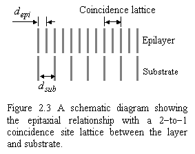
with respect to the substrate reference lattice. Continuum elasticity theory predicts that for small misfits, the epilayer can be initially grown pseudomorphically (strained) on the substrate. However, as the epilayer thickness increases, its elastic strain increases until it is sufficient to activate misfit dislocation sources, after which plastic relaxation occurs. This critical thickness at which misfit dislocations are generated varies approximately inversely with f . For large misfit systems, the assumption of elasticity theory is no longer valid and the breakdown of epitaxial growth is expected. Indeed, for systems with a mismatch higher than ~15%, the growth often results in polycrystalline phase. Some exceptions of this rule are, however, found and can be explained by a coincidence site lattice (CSL), which is explained below [Trampert et al.]. True coincidence between the epilayer and substrate lattices would occur when depi/dsub= m/n, where m and n are integers, and depi and dsub are atomic distances of the epilayer and substrate, respectively. If m = n + 1, for example, there is one extra lattice plane, i.e., a simple edge dislocation (misfit dislocation) in each unit cell of the coincidence lattice. A simple lattice-model given in Fig. 2.3 illustrates clearly this epitaxial relationship.
The coincidence lattice mismatch d , which expressed the deviation from true coincidence, is given by
This deviation will also introduce elastic strain at the interface in addition to strain accommodated by misfit dislocations. Thus the energy of heteroboundaries is expected to be small if and only if d does not deviate substantially from true coincidence. |
||||
|
2.2.2 Substrates for GaN epitaxy Because bulk GaN crystals were not commercially available (now, commercial GaN wafer is available (f ~ 3 mm), yet it is still too expensive), GaN has been grown ‘heteroepitaxially’ on foreign substrates. Thus, the quality of the GaN epilayer is considerably dependent on the properties of the substrates as well as the onset (nucleation) of the film growth. The lateral (a-lattice constant) mismatch, for example, can cause high density of misfit dislocations, which is detrimental for the device performance, causing high device leakage current, short minority carrier lifetime, reduced thermal conductivity etc. [Liu et al.]. A non-polar substrate can also give rise to mixed polarity in the epitaxial film and formation of inversion domains. The important parameters of the substrates include inherent properties such as lattice constants, thermal expansion coefficients and polarity, as well as process-induced properties such as surface roughness, step height, terrace width, and wetting behavior. Most commonly used substrates for the growth of GaN are sapphire (Al2O3), 6H-SiC, 3C-SiC, Si, GaAs, LiGaO2, and AlN [Liu et al.]. For homoepitaxial MBE growth, a GaN template, grown by MOVPE on Al2O3, has been used since bulk GaN is only available with mm-size [Kaschner et al.; Fernandez et al.]. Recently, new techniques such as pendeoepitaxy (PE) or lateral epitaxial overgrowth (LEO) have demonstrated that regions of lateral growth exhibits four to five orders of magnitude lower density of dislocations compared to regions of vertical growth [Zheleva et al.]. Detailed information about the substrates for the GaN growth can be found in the review by Liu et al. Table 2.2 summarizes the lattice mismatches f between III-nitrides and several commonly used substrates. The GaN epilayer grown on sapphire (0001) is found to grow with 30° rotation with respect to the substrate, resulting in a significant decrease of the lattice mismatch from ~33% to ~15%. In the next section 2.2.3, a detailed description on the sapphire substrate and its particular epitaxial relationship to III-nitrides will be given. |
||||
|
Table 2.2 Lattice constant difference, f (%), between III-Nitrides and some most commonly used substrates. (-) sign represents compressive strain. |
||||
| Interface | f (%) | 30O-rotation | ||
|
a-AlN/(a-Al2O3) |
34.6 % |
13.3 % |
||
|
a-GaN/(a-Al2O3) |
33 % |
14.8 % |
||
|
a-InN/(a-Al2O3) |
25.8 % |
14.6 % |
||
|
a-AlN/(6H-SiC) |
(-) 1 % |
|||
|
a-GaN/(6H-SiC) |
(-) 3.5 % |
|||
|
a-InN/(6H-SiC) |
(-) 14.6 % |
|||
|
GaN/AlN |
(-) 2.5 % |
|||
|
b-GaN/(001) GaAs |
20 % |
|||
|
a-GaN/(111) GaAs |
20.2 % |
|||
|
a-InN/(111) GaAs |
11.7 % |
|||
|
b-GaN/(001) Si |
16.8 % |
|||
|
a-GaN/(111) Si |
16.9 % |
|||
|
a-InN/(111) Si |
8.1 % |
|||
|
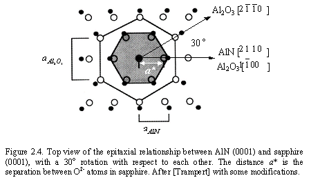
2.2.2 Sapphire for AlN epitaxy AlN is a most commonly employed buffer layer for the growth of GaN on sapphire substrate. The in-plane lattice mismatch between AlN (0001) and sapphire (0001) is given by f = (aAl2O3 - aAlN)/aAl2O3 = 0.35, which is an enormously large value so that epitaxy cannot be expected. Fortunately, when the AlN (0001) is grown on sapphire (0001), it rotates 30 ° about its c-axis with respect to that of sapphire, giving rise to the particular crystallographic relationship such as AlN
(0001) ||
Al2O3 (0001) and AlN [
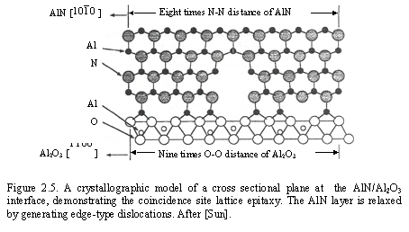
A schematic diagram showing this epitaxial relationship is given in Fig. 2.4. In this case, the atomic distance between the O atoms (a*) in sapphire is 2.747 Å, and Al-Al distance in AlN is 3.112 Å, thus the lattice mismatch in this orientation being significantly reduced to 13.3%. More interestingly, this epitaxial relationship leads simultaneously to a coincidence site lattice. From the value 2.747 and 3.112, the smallest nonreducible integral ratio between them is 8:9. Therefore nine times (n = 9) the O-O distance of Al2O3 is nearly equal to eight times (m = 8) the Al-Al distance of AlN. This is well illustrated in the crystal growth model suggested by Sun et al. (Fig. 2.5). The coincidence lattice mismatch is, thus, obtained from the Eq. 2.2.2 as d = 0.70% (the epilayer under tensile strain). This low d-mismatch may be responsible for the epitaxial growth (alignment), and thus for the relatively good crystalline quality obtained in AlN/sapphire or GaN/sapphire epilayers. Experimental confirmation of this epitaxy assisted by the coincidence site lattice is found in the report by Ponce et al. They observed a regular misfit dislocation distance of 2.0 nm in the AlN/Al2O3 interface using high-resolution transmission electron microscopy technique. |
||||
|
|
||||
|
|
||||
|
References:
A. Trampert, O Brandt, and K. H. Ploog, Chapter 7, Crystal structure of Group III Nitrides, Vol 50 (Academic Press, 1998) L. Liu and J. H. Edgar, Materials Sicence and Engineering, R 37, 61 (2002) A. Kaschner, et al., MRS Internet J. Nitride Semicond. Res., 5S1, W11.34 (2000). S. Fernandez, F. B. Naranjo, F. Calle, M. A. Sanchez-Garcya, E. Calleja, P. Vennegues, A. Trampert, and K. H. Ploog, Appl. Phys. Lett., 79, 2136 (2001). T. S. Zheleva, W.M. Ashmawi, and K.A. Jones, Phys. Stat. Sol. (a), 176, 545 (1999). C. J. Sun, P. Kung, A. Saxler, H. Ohsato, K. Haritos, and M. Razeghi, J. Appl. Phys., 75, 3964 (1994). F. A. Ponce, J. S. Major, W. E. Plano, and D. F. Welch, Appl. Phys. Lett., 65, 2302 (1994). |
||||
|
|
||||