
The c-axis (or out-of-plane) coupling has become especially important when the interlayer tunneling model of HTS has been developed. In this model, the energy gain that drives the formation of the pairs is associated with a decrease of the kinetic energy due to the easy motion of the pairs accompanied by the impeded single-particle tunneling along the c-axis.
Another important question is whether the normal state out-of-plane transport is coherent or not, and what is the origin of the "semiconducting" c-axis resistivity in the cuprates. All theories of out-of-plane transport differ in whether the zero-temperature state of cuprates is "metallic" with a finite c-axis resistivity rc, or insulating with an infinitely large rc. Major c-axis transport models have been examined in the review article by Cooper and Gray.
The physics of vortices has become one of the most quickly developing part of modern physics. HTS's with their large anisotropy and thermal fluctuations represent a big research field where many new effects have become possible to observe experimentally. A clear experimental evidence for melting of the classic Abrikosov vortex lattice in a wide temperature range below superconducting critical temperature Tc has verified a number of theories and stimulated further experimental and theoretical studies.
Intrinsic Josephson effect (IJE) as a tunneling of the Cooper pairs between adjacent CuO2 planes inside the highly anisotropic layered HTS is an integral part of almost all theories on this subject and is of primary importance for deriving the properties of the vortex system. It was experimentally confirmed by Kleiner and Müller, that the intrinsic tunneling of the Cooper pairs indeed takes place in Bi2Sr2CaCu2O8+d(Bi-2212) and other anisotropic single crystals (Tl2Sr2Ca2Cu3O10+d(Tl-2223) and (PbyBi1-y)2Sr2CaCu2O8+d(Bi(Pb)-2212) ). In these experiments both dc and ac Josephson effects have been observed. The current-voltage (I-V) characteristics for current flow in the c-axis direction exhibited large hysteresis and multiple branches. These results clearly showed that all the materials behave like stacks of superconductor-insulator-superconductor (SIS) Josephson junctions, see Figure below. The review of all these observations and the present status of research regarding theoretical understanding of the intrinsic Josephson effect has been given some time ago. For an unsorted collection of recent works on intrinsic Josephson effect, see this Reference.
The experimental discovery of IJE in HTS's is very important because it sets in the limitations on possible theories of HTS and requires reassessment of many works. Those experimental works which involve the c-axis tunneling in highly anisotropic HTS but fail to demonstrate IJE clearly, should be taken with discretion.
One of the important issues of HTS is its promising practical applications, like three-terminal devices or SIS mixers. Attractive feature of HTS's, their large energy gap in the quasiparticle excitation spectra implies that the operational upper frequency for feasible HTS-devices may lie in the THz-region. Since the discovery of HTS, there have been worldwide attempts to obtain reproducible tunnel junctions of HTS materials for potential applications. The most popular and most developed Josephson junctions use different types of weak-link contacts between misoriented thin films of HTS, see discussion on the different types of HTS Josephson junctions. Although there are some signatures of SIS nature of, for instance, grain-boundary Josephson junctions, a well-defined quasiparticle gap feature which is a signature of the elastic, single-particle tunneling, is very seldom clearly observed. Moreover, the nature of the weak contact between misoriented grains of HTS is still unclear. Intrinsic Josephson junctions favorably stand out against other types of HTS Josephson junctions by their naturally perfect structure in terms of uniformity and reproducibility and their SIS character, which makes them attractive for device applications.

Taking the simplified scheme alone, we make conclusion that the whole Bi-2212 single crystal is just one-dimensional array of S-I-S Josephson junctions. We call such junctions as intrinsic because they are inside the singler crystal. We also believe they are unique and are the only example of naturally made Josephson junctions with extreme degree of quality and uniformity. Such an array has a current-voltage characteristic which consits of several branches when current is sweeping back and forth from zero to a some maximum value. Each branch corresponds to one, two, three etc. intrinsic Josephson junctions having switched to the dissipative regime (quasiparticle state) with a finite voltage across each of them, see Fig.2.

for details see A. Yurgens, D. Winkler, N. V. Zavaritsky, and T. Claeson, Appl. Phys. Lett. 70, 1760 (1997).
Motivation: The interlayer tunneling model (ILT) is one of the leading candidates for explaining
high-temperature superconductivity. In this model, the energy gain that drives
the formation of the pairs is associated with a decrease of the kinetic energy
due to the easy motion of the pairs accompanied by the impeded single-particle
tunneling along the c-axis. The model in its current version predicts an
increase of the condensation energy Ec proportionally to
the interlayer Josephson coupling t^2,
or to the inverse square of the c-axis penetration depth lc, or the c-axis critical current.
A conclusive experimental check of this prediction for different single-layer
high-Tc materials would provide a critical test of the ILT model.
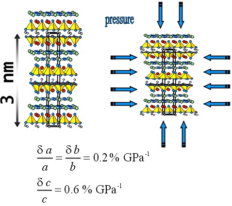
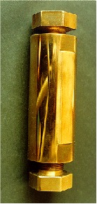
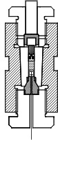
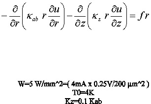
We used hydrostatic pressure P < 1 GPa as a tool to change the c-axis interlayer coupling of Bi2Sr1.5La0.5CuO6+x (Bi-2201) and Bi-2212 single crystals, see Fig. 4. The pressure can be applied in a simple pressure chamber, see the photo.
Results.
The c-axis critical current of Bi-2212 (left) and Bi-2201(right), as
a measure of the interlayer coupling, drastically increases with pressure
(up to 270 %GPa-1), see Fig. 5.
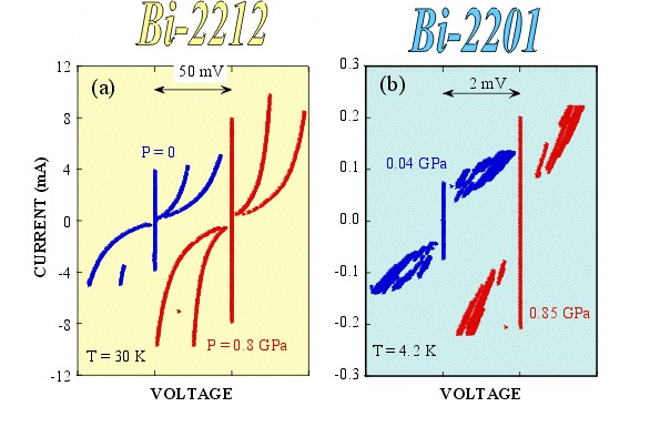 Fig. 5
The superconducting critical temperature, on the contrary, only slightly
increases with a rate of ~ 2-6 % GPa-1, see Fig. 6, the inset.
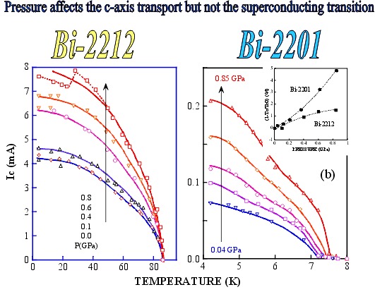 Fig. 6
Conclusions.
All this implies that the CuO-interlayer coupling has little effect on Tc in Bi-system, in contrast to the ILT model.
Measurements of the c-axis, out-of-plane, electrical transport properties
are of great importance in probing the vortex system properties of highly
anisotropic layered high-Tc (HTc) compounds, such as Bi2Sr2CaCu2O8
(2212-BSCCO). In such superconductors, vortex lines are formed from
vortex "pancakes" with circulating currents confined to the CuO2
planes. The pancakes interact with each other magnetically and via interlayer
Josephson coupling. In an ideal layered superconductor at low temperatures,
these interactions encourage pancakes to align perpendicular to the planes.
However, when the interlayer interactions are weak, thermal fluctuations
and local pinning centres cause misalignment. This leads to a loss in phase
coherence between adjacent pairs of superconducting planes and hence a reduction
in the critical current.
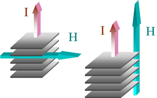
These orientations of the magnetic field, current, and the c-axis were used in our experiments.
Measurements of the field-dependent c-axis tunnelling characteristics
across the intrinsic interplanar Josephson junctions in epitaxial Bi2212 mesa
structures probe the interplanar pancake correlations on an atomic interlayer
length scale, complementing measurements of vortex correlations on the much
longer length scales involved in low angle neutron diffraction, mSR, magnetic, and bulk transport measurements.
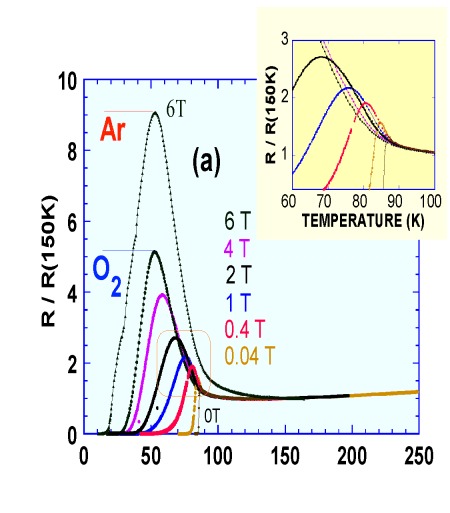
Temperature dependence of (a) the out-of-plane
resistances for the oxygen-annealed sample in a perpendicular magnetic field.
The inset shows an enlarged part of the dependence close to Tc.
For comparison, we have also included
a single 6- T measurement for the argon-annealed sample which exhibits a
resistance peak almost twice as large as for the oxygen-annealed sample, whereas
the zero-field critical current at low temperatures is approximately halved.
This suggests an inverse relationship between the magnitude of the resistive
peak and the critical current density.
Despite the onset of resistance at low voltages above Tirr,
it is still possible to define a critical current in terms of the "excess
current" extrapolated to zero voltage, which varies smoothly through the melting
transition regime, as illustrated in Fig. 4. The somewhat surprising existence
of a critical current extending well into the liquid state is a consequence
of the attractive Josephson or magnetic coupling of pancakes between the
planes. This results in a thermally averaged, partial alignment of the pancakes,
as described by Koshelev. This also accounts for the persistence of the microwave
Josephson plasma resonance at temperatures well above the irreversibility
line.
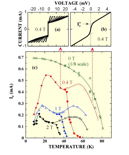
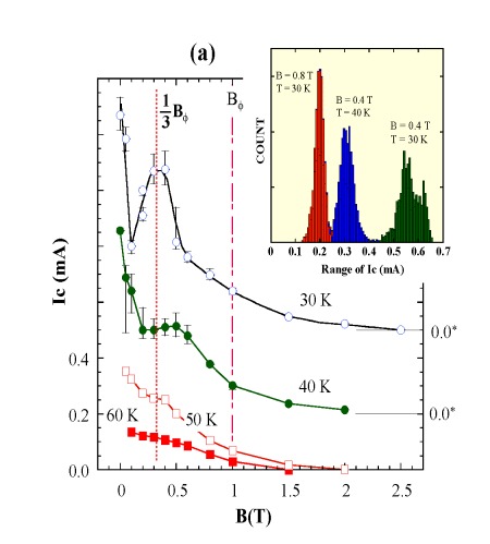
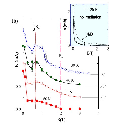
(a) and (b): I-V characteristics of the oxygen-annealed sample in the perpendicular magnetic field of 0.4 T at T = 36 K and T = 70 K.
(c) Temperature dependence of the
c-axis critical current for perpendicular magnetic fields as indicated. Empty
symbols represent the "quasi-critical" current Ic* defined
in Fig. (b). Filled symbols correspond to the critical current Ic defined
using a 0.1 µV voltage criterion or from the critical current distribution
functions P(Ic). The lines drawn through the experimental
points are only intended as guides for the eye.
Below, we show the B-T phase diagram suggested by our measurements for fields perpendicular to the ab-planes. The open symbols indicate the temperature T* of the first peak in critical current (see above) and the filled symbols the temperature Tirr marking the onset of resistivity along the c-axis. Over a relatively wide range of fields, Tirr µ ln(1/B^).
There appears to be a weak maximum in T* at small fields, while at large fields it approaches the field-independent, 2D vortex lattice Kosterlitz-Thouless melting transition, T2D. This is consistent with the suppression of both Josephson and electromagnetic interlayer coupling at high fields, so that the system becomes increasingly two-dimensional.
T* and Tirr define three regions of the B-T phase-diagram. This involves two solid phases below Tirr, where a zero voltage, true c-axis supercurrent is observed, and a liquid phase above Tirr, where the c-axis conduction is dissipative. T* may mark the temperature at which both C44 and C66, the elastic moduli of the vortex lattice, are predicted to vanish. The phase between T* and Tirr may represent a glassy state of vortices with long-range orientational order; whereas the transition to a more conventional liquid state does not occur until Tirr.
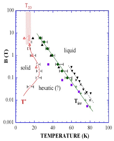
B-T- diagram of vortex phases for fields
perpendicular to the ab-planes suggested by our measurements. Empty symbols
represent the field dependence of the temperature T* at which the maximum
of Ic(B^,T)-dependence
is observed, see Fig. (c) above. The solid symbols represent the irreversibility
line Tirr(B^)
observed in different experiments:(? )- µSR measurements; (? )-melting
line from Ref. , where multi-terminal transport measurements in the flux-transformer
configuration have been made; (? ) and (+)- irreversibility line inferred
from the magnetization measurements of a 2212-BSCCO single crystal from the
same batch as those used in the present study (upper triangles and circles,
for the argon and oxygen annealed sample, respectively). Although the lines
are only guides for the eye, the irreversibility temperature seems to obey
a simple logarithmic dependence, Tirr(B^) ? -ln(B^), illustrated by the straight line in this
semi-logarithmic plot.
Although the rapid onset of a resistance at Tirr(B^)suggests a first-order melting transition,
as observed by Fuchs et al. at small fields, the absence of any qualitative
change in the I-V characteristics at the transition imply a second-order
or thermally broadened phase transition at these higher fields. Our measurements
suggest that there is little change in the correlation of flux pancakes in
the c-direction at the melting transition, with perhaps a significant
fraction of pancakes remaining strongly pinned at this transition. This could
also account for the slight increase of Ic*(T,B^) on increasing temperature above Tirr(B^) as such pancakes eventually become thermally
unpinned, enabling them to move more freely and hence to optimise their thermally
averaged alignment along the c-direction.
Figure shows Rc(T) at different magnetic fields for two samples before and after irradiation. First, it is seen (top panel) that the increase of the resistance for one of the samples (No.1) in merely 5 T of the field strength is about 60 times the normal state resistance at T=160K. Typically, we observe an increase of resistance of the order of (10-12)Rc(160K) in 6-7T. We believe that such a big magnetoresistance effect is due to an occasionally perfect Bi-2212 crystal structure in the investigated mesa. Crystalline defects would likely provide local electrical shorts between CuO planes, thus decreasing the overall sub-gap resistance Rsg of an individual IJJ. Recently, we have experimentally shown that Rsg sets an upper limit of the magnetoresistance peak effect (MRPE) of a Bi2212 single crystal. After irradiation with a total dose of ions of 1011cm-2 (corresponding to a matching field Bf=2T) MRPE is significantly suppressed to a value of 20, see the inset of Fig.(top). For the second sample (No.2) the change of the MRPE after irradiation is only 20%. This may be due to a lower dose (Bf=1T) and to a difference in sample quality (the MRPE for that sample was about 20Rc(160K) prior to irradiation). The temperature of the zero-resistance state, Tc(B), increased significantly after irradiation for both samples.
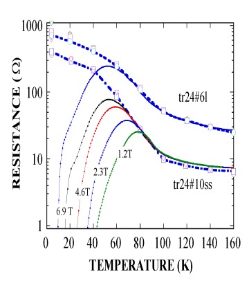
See also Fig. where the 60-fold increase
of resistance in the magnetic field of about 6 T was observed.
In Bi-2212 with rather poor thermal and electrical conductivity, the Joule heating at high bias current may become essential, and a short-pulse technique may be needed to overcome such a problem.
We have chosen another method, and have used intercalation
of the inert HgBr2-molecules to lengthen the c axis of the host
Bi-2212 single crystals, see Fig.7.
Correspondingly, the intrinsic tunneling barriers are becoming wider which
results in a drastic decrease of the c-axis critical current density.
In its turn, the heat-release during sweeping the current to reach the normal-state
tunneling parts of the current-voltage (I-V) characteristics drops off as
well.
Remarkably enough, such an intervention does not change quality of resulting
I-V's , which usually consist in evenly spaced in voltage hysteretic quasi-particle
branches. The total number of the branches seen in I-V-plot tells one how
many intrinsic Josephson junctions (IJJ) are enclosed in the mesa, see the
Figure below.
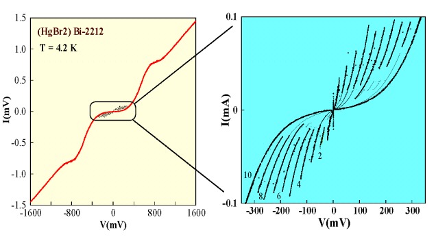
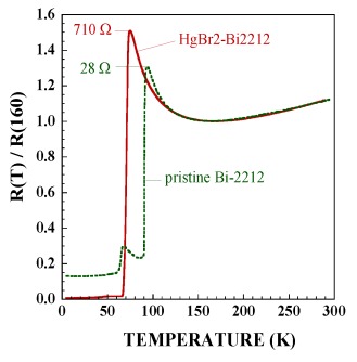
Figure shows the normalized resistance
R for both the pristine Bi2212-, and HgBr2-Bi2212-mesas of the same areas
and heights. It is seen, that the overall shape of R(T)-dependence
and the characteristic temperature T* at which an upturn in R(T)-
dependence sets in upon cooling do not change. This implies that T*
is not affected by the coupling between the CuO2-bilayers. Pseudogap-feature in
Bi2212 is thus derived from the properties of the bilayers alone. See also
intrinsic spectroscopy of the pseudogap below.
The tunneling spectroscopy is particularly sensitive to the density of states (DOS) at the Fermi level and therefore can be used to study any gap in the quasiparticle excitation spectrum. The most common experimental methods, STM and point-contact techniques are surface probes, and therefore are affected by surface deterioration.
In our experiments we study the tunneling properties of Bi-2212 using the so called intrinsic spectroscopy (Schlenga98), for which such problems are unimportant. The atomic perfection of the naturally occurring tunnel junctions in this material provides a reliable basis for the tunneling spectroscopy inside the single crystal giving a high degree of homogeneity and reproducibility.
The quasiparticle branches in Figure are having a well defined gap feature. For instance, the slope of the first quasiparticle branch is almost vertical at V»25 mV. The same applies for the last branch, too. Since it corresponds to all 9 IJJ in the quasiparticle state, one can deduce the average value of the gap voltage per junction to be about the same 25 mV. Recalling the fact that for the SIS-type Josephson junctions the gap feature is taking place at V»2D /e, we conclude that D» 12-13 meV for tunneling in the c-axis direction. This value is about one half of the value obtained from the scanning tunneling microscopy (STM) data, or break-junction technique.
Several explanations have been suggested. The trivial heating explanation (see Problems) implies that the temperature of the mesa is increased up to about 0.6Tc due to the power dissipation in the junctions. Assuming a BCS-like temperature dependence of the gap parameter, one would see then a smaller than expected gap. On the other hand, the more IJJ are going normal in the stack, the more heat power is released, and the less gap voltage and the smaller separation in voltage between branches with higher count numbers should be observed. It is contradicting the experiment, where almost all branches in the I-V-characteristics are equidistant in voltage.
The non-equilibrium quasiparticle self-injection, which is typical for stacks of tunnel junctions, can also cause the gap to decrease. Since the thickness of each electrode of individual IJJ is about 3Å only, the quasiparticles generated in one junction can easily penetrate others and change the quasiparticle population. The competition between the rate of generating of quasiparticles and their recombination rate determines the steady concentration of quasiparticles and the operational gap parameter.
The proximity effects suggested (we97) could explain both the reduced value of the gap parameter and its strong temperature dependence. If one assumes that the bottle-neck for the current flow in the c-axis direction resides in between adjacent BiO-layers, which can be metallic and even superconducting due to proximity effects, then the actual schematics of intrinsic tunnel junction is SS'-I-S'S rather than S-I-S. (S' here represents superconducting BiO-plane with a smaller superconducting energy gap), see Structure. The reduced and strongly temperature dependent energy gap has also been observed in angle-resolved-photoemission (ARPES) experiments (Ma??).
The results on the reduced value of the c-axis energy gap were criticized in the paper by Itoh \etal, where the authors also used the small-height stacks on the surfaces of Bi-2212 single crystals. In their three-probe measurements, Itoh \etal managed to reach the normal-state parts of the tunneling I-V-characteristics for which there were no parts with negative dynamic resistance. The S-shaped characteristics with heavy back-bending at the gap-voltage usually witness to the heating in stacks. To further decrease the heating in contacts to stacks the authors annealed them at 650ºC during 1h. Although the diffusion of the silver into the stacks during the annealing had most likely distorted the properties of the host material, it looks that the two works differ mainly in measurement techniques, as whether the three- or four- probe methods were used.
In the four-probe technique, where the current and potential leads are separated by a distance of several microns, the non-equilibrium effects are more prominent than in the three-probe measurements. Charge imbalance at high bias current can initiate an additional voltage at the top of the stack between potential and current leads. That is why it is seldom possible to reach the normal state in the four-probe measurements without the back-bending of the tunneling curves. Moreover, the high bias current accompanied by non-equilibrium effects which are present in all cases, may destroy the weak superconductivity of BiO planes and make the corresponding reduced gap unobservable. At low currents, the results of three- and four- probe measurements are basically similar, and the separation in voltage between the branches is the same 20-30 meV.
Pseudo-gap (PG) in electronic excitation spectra is one of the very important
features of high-Tc (HTS) superconductors. Such a gap was reported
to exist in both underdoped and overdoped samples, and was observed to transform
into the superconducting gap (SG) upon cooling in a number of experiments
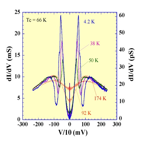
Figure shows the c-axis dynamic
conductance dI/dV(V) for HgBr2-Bi2212 at
different temperatures, obtained by differentiating the last branch corresponding
to all 14 IJJ being in the quasi-particle state. Both SG- and PG- features
are clearly resolved at T<Tc and are therefore
concluded to be independent phenomena. Moreover, the PG-feature does
not depend on temperature, while SG-voltage decreases with T and looses
its distinctiveness on approaching Tc. For slightly underdoped
HgBr2-Bi2212, SG-feature could be traced closer to Tc
than for the similar overdoped crystals. Note also that, being re-scaled
down to areas 5x5 Å2 which may be presumed for STM, the
conductance results in even smaller than in STM values 10-12 Ohm-1.
This proves the high quality of intrinsic tunnel junctions.
![]()
K. Schlenga, et al., Phys. Rev. B 57, 14518 (1998).
The main problem with intrinsic Josephson junctions seems to be the intrinsic
overheating at high bias.
Almost all high temperature superconductors have a low thermal conductivity,
which easily makes them overheated locally. For instance, taking the thermal
conductivity k ~10-2 Wcm-1K-1,
geometrical factor L~10-3 cm (assuming the typical area
S of mesa ~100 µm2 and the thickness of a single
crystal L~10µm), we obtain the thermal conductance of about
10-5 WK-1. Even for a low dissipation level of about
1 mW (for I» 3 mA and V»300mV, corresponding to the sum-gap voltage
of about 10 IJJ) we immediately have the overheating dT~100K.
The overheating is one of possible reasons for the "back-bending" of I-V-characteristics at high bias current, see Figure. When the temperature of the stack is increasing with bias current and approaches Tc, the temperature dependent energy gap parameter becomes smaller. Accordingly, the sum-gap voltage decreases also. The experimentally obtained reduced 2D» 25meV may therefore be a result of trivial overheating.

Since the 1950's, when study of the superconducting three-terminal devices started with cryotrons, much attention has been paid to their development (Bremer). The interest in superconducting transistors is due to their potential advantages, like the ability to sustain high controllable current densities without energy dissipation. Moreover, superconducting transistors are compatible with other superconducting components, and may be required to interface with superconducting electronics. Research on the superconducting transistors has been intensified since the discovery of HTS, which opened ways of making relatively cheap devices operating at liquid nitrogen temperatures. There have already been made many attempts to fabricate different types of HTS transistors (Mannhart, Claeson). The main types of superconducting transistors are: Josephson vortex flow transistors , electric field-effect devices (SFETs), and quasiparticle-injection devices. They have been shown to work at liquid nitrogen temperatures and to have finite current or voltage gains.
Intrinsic Josephson junctions have an attractive feature of their SIS- character of current-voltage characteristics, which opens up roads for possible application like making heterodyne (SIS) mixers. The wider energy gap of the high-Tc material may increase the operation of SIS mixers up to about 5 THz. Other interesting features are the extremely small thickness of the electrodes of each junction and the easiness of making stacks of different areas and heights. The latter is in a favorable contrast to all other types of high-Tc Josephson junctions, for which the fabrication of stacked planar structures has always been a problem. This makes this material promising for three-terminal devices, as will be explained below.
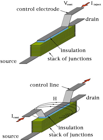
Quasiparticle-injection devices
The principle of such devices refers to the injection of non-equilibrium quasiparticles into the drain-source (DS) channel from the control electrode through a tunnel junction or weak link, formed on top of the DS channel. The interest for these devices arises from a potential current gain and a fast response time due to the creation of a non-equilibrium state. The characteristic times of the relaxation of such a state is of the order of 1-100 ps (Mannhart).
Figure (a) schematically shows the assumed arrangement of such a device with intrinsic Josephson junctions. The thickness of the electrodes, which make the Josephson junctions in the Bi-2212 single crystals is extremely thin, 3 Å. This means, that the injected high-energy quasiparticles can penetrate several unit cells deep into the Bi-2212 single crystal from its surface and influence the properties of many intrinsic Josephson junctions connected in series. This promise to increase the sensitivity and performance of a device involving many IJJ.
The change of the density of quasiparticles dn=n-n0(T) due to the current injection is:
dn=jt/ed
where j is the injection current density, t is the effective recombination time, e is the electron charge, d is the quasiparticle penetration depth, n is the total density of quasiparticles, and n0(T) is the thermally excited density of quasiparticles. Taking j~103 Acm-2, d~10-100 Å, corresponding to the mean free path of quasiparticles, and t~1-100 ps, we get dn~1010-1011 cm-3. This value has to be compared with n0(T). For a BCS superconductor, this number is exponentially decaying with decreasing of temperature, n0(T)µ exp(-D/T). To get n0(T) of the same order of magnitude as dn, one has to work at low temperatures. Estimations show that the temperature should be less than 20-30 K for such a quasiparticle-injection device to work. The most indefinite parameter in this consideration is the effective recombination time t and the mean free path of quasiparticles.
For quasiparticles injected at much higher, than D
energies this time involves the electron-phonon relaxation and phonon escape
times due to the avalanche-like creation of the secondary quasiparticles,
including phonons. These times are usually several orders of magnitude higher
than t~1-100 ps, used for the above estimation.
This may drastically improve the low-frequency characteristics of the device
at high temperatures ~70 K, but, unfortunately, decrease the cut-off frequency
down to 1 - 10 GHz. One should therefore find the optimum between speed,
working temperature, and responsivity of the device. The parameter to change
is simply the thickness of the insulation layer between control electrode
and the stack of intrinsic Josephson junction. The thicker the layer the
higher is energy of the injected quasiparticles and the more avalanches of
the secondary quasiparticles are generated, which makes the responsivity
higher. This however may slow down the speed as it takes longer time to get
rid of all these quasiparticles afterwards for restoring the initial state.
The Bi-2212 IJJ are hysteretic at low temperatures and one can possibly make
use of this feature by fabricating switching devices also. Number of junctions
N which can feel the injected quasiparticles may be of the order of
10-100, so the output voltage of such a device can be 2DN~0.1-1 V without additional amplification.
Electric field-effect devices.
An electric filed applied to a superconductor via an insulating barrier changes the density of the Cooper pairs in a thin layer of the depth d of the superconductor close to the superconductor-insulator interface. As the pair potential of the superconductor is a function of the Cooper pair density, all superconducting properties in the field-penetrated layer depend on the applied electric field. The characteristic length, which has to be compared to the field-penetrated depth d is the superconducting coherence length x . The condition d³x(T) should be satisfied for the effect of the applied field be seen in the superconducting properties of the DS channel. In the majority of high-Tc superconductors, d is of the order of 1-10 nm (Frey95, Mannhart96) and x (T) is of the same order, in contrast to low-Tc ones, for which d<<x (T), and the field effects are small.
The arrangement of the suggested IJJ-FET transistor is the same as for the quasiparticle-injection one. The only difference is that the insulation layer between the control electrode and the stack should be made much thicker to have basically no input current between the two. This is promising for achieving a high current gain. Intrinsic Josephson junctions incorporated in such a type of devices favorably feature in comparison to all other high-Tc junctions by their planar layered structure and their having a short coherence length in the c-axis direction. As compared with the previous work (Frey95), the suggested IJJ-FET is more feasible because all affected by the electric field junctions contribute to the output voltage, and even one of IJJ is enough for the device to be operate.
Moreover, in the usual in-plane geometry (Frey95, Mannhart96), the superconducting sheets which are further away from the gate electrode and which are less affected by the field, just short electrically the "useful" ones. Therefore the field-response of thick layers of HTS material is basically much smaller than that for a thin layer ~10 nm.
Josephson vortex flow transistors
In such devices, a drain-source (DS) channel is formed by a long Josephson junction or by a number of short Josephson junctions connected in parallel. The control line is usually put close to the channel, and the magnetic field induced by the current in the control line generates Josephson vortices in the junction. The vortices suppress the critical superconducting current Ic of the junction, and once they flow under the influence of the drain-source current IDS, they change the junction resistance. Such transistors could have excellent decoupling of the input circuit from the output one and no may operate at frequencies of the order of 500 GHz (Mannhart). A simplified schematics of the suggested device is drawn in Figure (b). There is a stack of 10 - 100 intrinsic Josephson junctions with contacts on the top and near the base of the stack (drain and source). The lateral dimensions are chosen with a big aspect ratio to form the so called "long" Josephson junction with the in-line geometry. Dimensions of the stack, which can be used for estimations are 100x2x0.05 µm3. There is also a control line on top of the stack, made from a thin metal film, and which is electrically isolated from the stack. In this geometry, the control current Icont applied to the line produces a magnetic field, which, once becoming larger than the first critical field Hc1, generates the Josephson vortices in the stack. Hc1»10 G for the Bi-2212 material. This value agrees with experiments on vortex flow in long stacks of IJJ (Lee95).
The current Icont in the control line, which is needed
to induce such a magnetic field in the stack may also be estimated from the
formula 4pIcont/cw, where
c is the velocity of light and w is the width of the control
line. Taking w~2µm, we get Icont~1 mA. This
means that just small currents are sufficient to control the vortex motion
in the stack for the simplest geometry of the device. To further improve
the sensitivity of the device one can use several layers of the control line
forming a multi-turn flat coil. It will increase the sensitivity but will
at the same time increase the input inductance and slow down the device.
The optimum matching to the external circuits must be found at high frequencies.
More? Please send me URL for including here.
Your comments will be greatly appreciated, too.

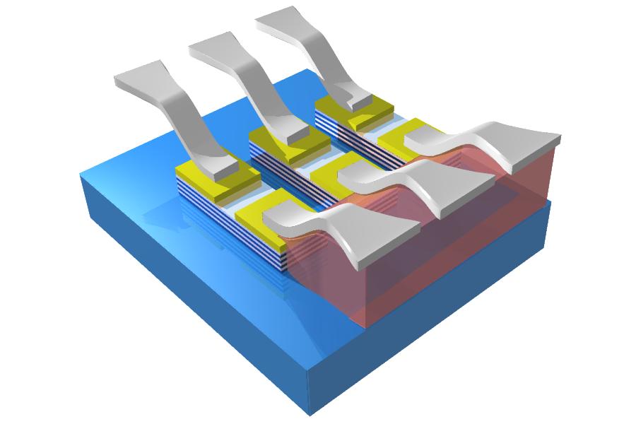
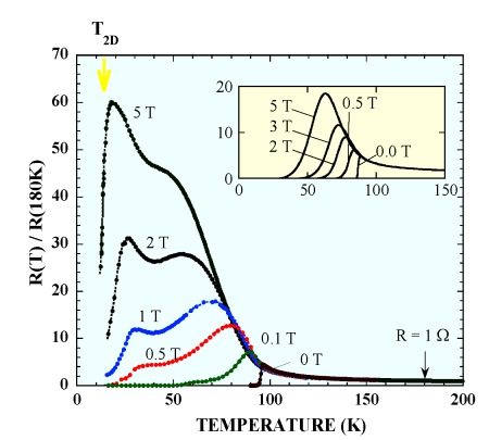
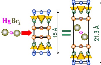 Fig. 7