Electron cooling in a normal metal hot electron microbolometer
M.Tarasov, L.Kuzmin, M.Fominsky, I.Agulo, A.Kalabukhov
Chalmers University of Technology
A capacitive coupled normal metal hot electron microbolometer (NHEB) with two superconductor-insulator-normal metal (SIN) tunnel junctions for electron cooling and two SIN junctions for temperature sensing have been fabricated and experimentally studied. By SIN junctions electron cooling that is analog to Peltier effect in semiconductors it is possible to reduce the electron temperature of such bolometer. Effective electron temperature was estimated from the ratio of dynamic resistance at zero bias to the normal state resistance. At the bath temperature 250 mK the resistance ratio of a 30 kW sensor junction pair approaches 1000 that is pretty close to theoretical value for this temperature. Applying the bias voltage nearly 0.4 mV to the external junctions of larger area brings increase in the zero bias resistance of central smaller junctions from 12 MW to 36 MW that corresponds to temperature decrease by 55 mK. The observed temperature response of the bolometer about dV/dTph=2 mV/K corresponds to electron temperature 200 mK. Electron cooling in bolometers reduces influence of a background power load and improves bolometer performance.
Motivation
Normal metal hot electron bolometer with capacitive coupling (CCNHEB) was proposed in [1] and experimentally demonstrated in [2]. Responsivity and noise equivalent power (NEP) of the bolometer are mainly determined by its electron temperature. To improve CCNHEB performance we suggest using electron cooling by a superconductor-insulator-normal metal (SIN) tunnel junction [3]. The direct electron cooling was demonstrated in [4] and further developed in [5].
For estimation of the actual electron temperature easiest way is to fit IV curve of a real junction by ideal SIN tunnel junction IV curve
![]() (1)
(1)
in which T is temperature, Tc is critical temperature of superconductor, e – electron charge, k – Boltsman constant, V – voltage. A subgap current can affect both shape of IV curve and electron temperature of the bolometer. Such subgap residual conductivity can be due to imperfectness of the tunnel barrier, normal inclusions in superconductor, etc. Another mechanism of subgap conductivity is two-electron tunneling when two normal electrons can be converted into a Cooper pair. The current will be much smaller compared to ordinary one-electron current [6]. Depending on junction geometry, the subgap conductivity is strongly enhanced if the interference effect is essential. It was also mentioned [7] that reducing insulator thickness and resistivity of junction leads to increase of Andreev reflections A(E),
 ,
, 
- single electron transmission coefficient, T – transmittivity, R – reflectivity. They assume Ubarr/D=100, and in real junctions usually Ubarr/D=104. According to their conclusion, such effect does not affect performance of cooler. Another effect is back-tunneling that can dominate at temperatures below 200 mK [8]. Without trap the cooling power is reduced due to electrons that return back to the normal metal. Some experiments [9] demonstrated temperature saturation below 300 mK when hot electrons are confined in the normal metal trap.
For practical junctions very important can be presence of a pinhole-type defect in tunnel barrier. Such defect is easy determined by residual conductivity at zero bias. For typical junction with normal resistance 1 kW at 350 mK the dynamic resistance at zero bias should be over 1 MW and we can take as example the leakage resistance of about the same 1MW. The electron temperature under absorbed power is estimated as
![]() (2)
(2)
in which P is absorbed power, S=3.109 Wm-3K-5 is metal parameter, V=0.18 mm3 is volume of absorber. For zero phonon temperature at standard dc bias of 400 mV the temperature is increased by about 200 mK. Even if bias voltage is 4 times as low, at 100 mV the temperature increase is still 115 mK. Increased by one order of magnitude leakage resistance to 10 MW does not help much and still brings temperature increase by 127 mK at 400 mV. It means that even small probe current increase electron temperature over equilibrium phonon temperature and calibration of electron temperature become rather tricky. Let us consider the zero-bias resistance ratio as electron temperature probe. Adding to equation (1) the parallel conductance of leakage current one can obtain the temperature dependence of zero-bias resistance of real junction
 , (3)
, (3)
in which Rn is normal resistance and Rs is shunting leakage resistance. Example of such dependence is calculated in Fig. 1 for parameters of one of our samples.
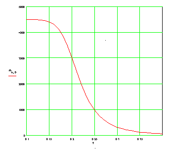
Figure 1. Zero bias resistance ratio calculated for sensor normal resistance Rn=10 kW and leakage resistance 45 MW.
For estimations of effective
electron temperature another simple figure of merit can be a temperature
responsivity dV/dTe.
According to [9] if the IV curve of SIN junction can be approximated as ![]() where
where 
The maximum temperature sensitivity is at zero bias
![]() (4)
(4)
In experiment we can measure dV/dTph so the dependence dTe/dTph should be added to the practically measured value to extract the required electron temperature.
As example in Fig. 2 is presented a temperature dependence of voltage for different bias currents from 0.12 pA up to 128 pA. Here we accounted for overheating and shunting the actual high dynamic resistance of SIN by leakage resistance.
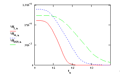
Figure 2. Temperature dependence of voltage across the 1 kW junction calculated for bias currents 0.12 pA, 8 pA, and 128 pA. Background power load is 1 fW, self-heating is accounted across 1 MW resistance.
Experimental
The illustration for that could be example of dynamic resistance of sensor junctions at different cooling voltages measured at 20 mK. One can see that the largest resistance of 45 MW is observed only at cooler zero bias. With any other voltage via refrigerator the resistance is below 37 mW that corresponds to electron temperature above 187 mK. In all other cases it is reduced. Large increase of sensor resistance at 250 mV with cooling bias 400 mV can be explained as cooling down from overheated level of over 187 mK. The same dependence measured at 250 mK (see Fig. 5) shows increase of a zero-bias sensor resistance from 12 MW to 36 MW with increase of cooling bias. It means that achieved by cooling the electron temperature difference is approximately the same in both cases. The resistance of junction in this case is not so much shunted by leakage and temperature can be estimated with high accuracy from the resistance ratio dependence calculated for shunted SIN junction according to equation (3). This temperature dependence is presented in Fig. 6.
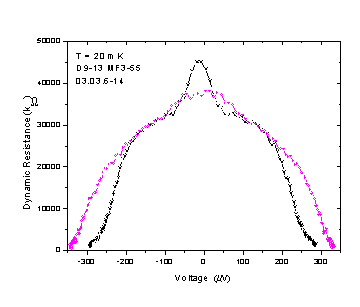
Figure 4. Dependencies of dynamic resistance of sensor junction on its bias voltage measured at 20 mK for cooling junction voltage up to 450 mV.
Figure 5. Dynamic resistance of sensor junction measured as dependence on bias voltage of cooling junction at 250 mK bath temperature. Largest cooling is observed for V=400 that brings Rzb=36 MW zero-bias resistance for cooling junctions. Without cooling Rzb=12 MW.
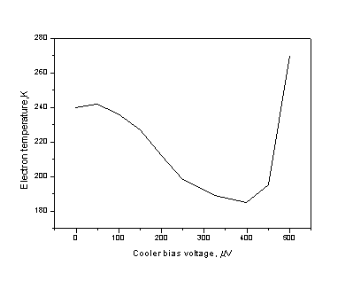
Figure 6. Equivalent electron temperature corresponding to the zero bias resistance ratio from Fig. 5 and calculations from Fig. 1.
Discussion.
The performance of bolometer is strongly affected by external overheating from the background power load and also from normal conducting channels in the tunnel barrier itself. The actual electron temperature without electron cooling can have excess level above the phonon temperature of the order of 100 mK. The electron cooling is even more effective when starting from enhanced temperature. In Fig. 7 one can see the electron cooling down by 66 mK starting from equivalent electron temperature 530 mK. The achieved response value for bolometer dV/dTph=2 mV/K.
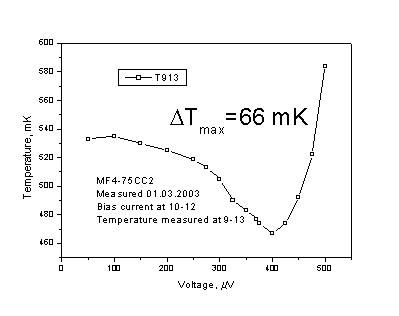
Figure 7. Electron cooling from 533 mK down to 467 mK.
We can numerically model both processes of overheating via shunting resistance plus background power load and electron cooling. The simplified analytic expression for cooling power is
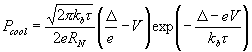
and the effective electron temperature t is
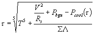
in which T is phonon temperature, V is dc bias voltage, Rs is shunting resistance, Pbgn=0.5hfDf=6.10-14, S=3.109 is material parameter, L=1.8.10-19 is absorber volume. The example of calculation according to these relations is presented in Fig. 8.
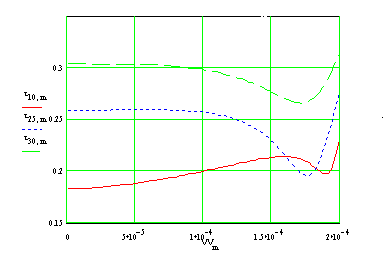
Figure 8. Electron temperature calculated for 100, 250 and 300 mK phonon temperature, Rn=1.8 kW and Rs=300 kW.
For bath temperature 100 mK one can see that at the beginning temperature is increasing up over 200 mK and then goes down to about 190 mK. The largest cooling effect of about 70 mK is observed at 250 mK phonon temperature.
In our junctions the maximum temperature responsivity at phonon temperature 260 mK was 2 mV/K, which corresponds to the electron temperature 200 mK. For low-resistive junctions with substantial electron cooling or at lower temperatures the response could be even higher and can be a figure of merit for the actual electron temperature like the zero-bias resistance ratio. To increase accuracy of this estimation the dependence of electron temperature on phonon should be accounted. Calculated dependence of dTe/dTph is presented in Fig. 9. One can see that in the case of strong electron cooling the correction factor can be over 2 times.
Figure 9. Dependencies of dTe/dTph on bias voltage for phonon temperatures 100, 230 and 300 mK.
Conclusion
We have designed, fabricated and measured a normal metal hot-electron bolometer with electron cooling. Electron cooling allows increasing the dynamic resistance and response of the bolometer. For estimations of effective electron temperature the ratio of zero-bias resistance to the normal resistance can be used as well as the voltage to temperature responsivity. Both figures of merit accounts for electron cooling and parasitic overheating.
Acknowledgements
Authors acknowledge support from INTAS-01-686, STINT
References
1. L.Kuzmin, On the concept of a hot-electron microbolometer with capacitive coupling to the antenna, Physica B, 284-288 (2000), 2129-2130.
2. M.Tarasov, M.Fominsky, A.Kalabukhov, L.Kuzmin, Experimental study of a normal-metal hot electron bolometer with capacitive coupling, JETP Letters, v. 76, N 8, 2002, pp. 507-510.
3. L.Kuzmin, I.Devyatov, D.Golubev, Cold-electron bolometer with electronic microrefrigeration, Proc. Of SPIE, v. 3465, pp. 193-199 (1998).
4. M.Nahum, T.M.Eiles, J.M.Martinis, Electronic
microrefrigerator based on a normal-insulator-superconductor tunnel junction,
Appl. Phys. Lett., v. 65, N 24, 3123-3125 (1994).
5. M.Leivo, J.Pecola, D.Averin. Efficient Peltier refrigeration by a pair of normal metal/insulator/superconductor junctions, Appl. Phys. Lett., v. 68 (14), 1996-1998 (1996).
6. F.W.J.Hekking, Yu.Nazarov, Subgap conductivity of a superconducting-normal tunnel interface, arXiv:cond-mat/9302034 v1, 23 Feb. 1993, pp. 1-12.
7. A.Bardas, D.Averin, Peltier effect in
normal-metal-superconductor microcontacts, Phys. Rev. B, v. 52, N 17 (1995),12873-12877.
8. J.Jochum,
C.Mears, S.Golwala, B.Sadoulet, J.P.Castle, M.F.Cunningham, O.B.Druru, M.Frank,
S.E.Labov, F.P.Lipschultz, H.Netel, B.Neuhauser, Modelling the power flow in
normal conductor-insulator-superconductor junctions, J.Appl. Phys., v. 83, N 6,
(1998), 3217-3224.
9. D.Quirion, F.Lefloch, M.Sanquer, Transport and heating effect in proximity superconducting structures, Physica E, 12 (2002), pp. 934-937.