 (1)
(1)
The operating point of the cascode can be set with three trim potentiometers located at room temperature. The source of Q1 is connected via a DC line to a 5 kohm trimmer in series with a 100 ohm resistance. This trimmer sets the drain current of Q1 as can be seen from inspection of the gate-source network. The 100 ohm series resistance provides a simple way of monitoring the drain current by measuring the voltage drop across it. The bias network is capacitively bypassed to ground to increase the gain. A bias network is connected to the Q1 drain - Q2 source node. It consists of a 50 kohm trimmer which can be used to set a different drain current in Q2 than that in Q1 making it possible to trim the DC bias at the output for optimum dynamic performance. It was necessary to insert a 5 kohm protection resistance in series with the trimmer since many JFETs burned up due to forward biasing of the gate-source p-n barrier. This protection found to be satisfactory. Finally, the gate of Q2 is biased by a 5 kohm trimmer. This trimmer sets the drain-source voltage of Q1. A parallel capacitance bypasses the trimmer to ground.
The cascode is followed by three non-inverting op-amp stages which together provide a gain of 400. The op-amps used were all OPA637 from Burr-Brown which need a gain greater than five to be stable. The first two stages each have a gain of 50, while the last has a gain of 8. The gain-bandwidth product of these amplifiers is 80 MHz, yielding a cut off frequency at 11.3 MHz for the first two and 10 MHz for the last stage. Inserted between each stage is a high-pass RC network, with a corner frequency of about 0.2 kHz. They remove DC components and eliminates the need for offset trimming the op-amps. Since the capacitors are in the signal path they are polypropylene types in order to get a good high-frequency performance. Two outputs with different gains are available; 250 and 2000. It was required to isolate the op-amp outputs from the capacitive loads that coaxial cable make up. The added capacitance adds a phase-shift to the negative feed-back making the amplifier unstable. An isolation of 50 ohm sufficed, and also resulted in matching the outputs to 50 ohm loads.
All power supply connections are in series with a 1 µH RF choke and shunted with 4.7 µF parallel with 100 nF to ground. The 4.7 µF are electrolytic types buffering large surge currents and the 100 nF are polystyrene types providing a good short-cut to ground for transients. Originally the RF chokes were 1.5 mH but they formed a LC tank with the shunting capacitors. The resonance frequency was about 10 kHz and modulated the power supply leads which was first detected as a peak in the frequency response. The modulation was checked with an oscilloscope connected to the power supply lines and a 10 kHz signal applied to the signal input. This indicates that rejection of power supply noise by the cascode is poor, which probably stems from the low output impedance of the MESFET making the source bias circuit susceptible to power supply variations. The 1 µH chokes removed the 10 kHz resonance. Protection diodes were inserted in between the power supply pins. The diodes are reverse-biased under normal operating conditions. If the applied voltage is reversed the diodes are forward biased, conducting heavily. The resulting current surge will burn the power supply's fuse removing the voltage (The fuse must of course have a lower current rating than the diodes).
Fig. 2-1. The circuit schematics. The inputs are labeled IN+ and IN- and the outputs x 250 and x 2000. Components within the dashed box are situated at cryogenic temperature.
2.2 The cascode
The cascode configuration is a circuit providing a large bandwidth (which shouldn't be confused with the cascade configuration). The circuit eliminates the so called Miller effect which is the capacitive feedback from drain to gate electrode of the FET. This effect limits the upper frequency in a common-source circuit. The Miller effect and the Cascode are extensively discussed in ref. [6] .
Lee describes a cryogenic preamplifier using GaAs MESFETs in a cascode [5] . It consists of a cryogenic part containing MESFETs in parallel connected by a coaxial cable to a room temperature part with a common Si JFET completing the cascode. The cascode is followed by conventional op-amp stages. The gain of the cascode is given by
where gm is the transconductance of the MESFET, r0-cs is the drain output impedance of the MESFET, rs-2 and r0-2 are the source input impedance and the drain output impedance of the JFET respectively, and Rd is the resistor at the drain of the JFET.
2.3 Experimental Apparatus
Physically the amplifier is made up of three parts, the cryogenic electronics contained in 'the cold box', the room temperature electronics contained in 'the warm box' and a dipstick connecting the two boxes. With the boxes mounted on the stick, the cold box can then be inserted in a 2" neck helium dewar. The cold box must be shielded and must be small enough to fit inside the cryostat. The dipstick must be a poor heat conductor to conserve liquid helium but yet present a low electric resistance for the signals. The warm box must be shielded to avoid interference.
The cold box, shown in Fig. 2-2 , was milled from a brass block. Two SMA connectors connects to the input terminals of the amplifier. The SMA connects their centers to the gate and signal ground respectively. The signal ground is thus separated from the chassis (See also section 2.4 ). Because the MESFETs came four per package, jumpers were installed to be able to connect each MESFET independently. Another pair of jumpers makes it possible to connect/disconnect the test signal leads to the amplifier input. The drain of the MESFET is connected to the center lead of a coax. The shield of the coax is connected to signal ground. The source of the MESFET is connected to a DC line. The coaxes and DC lines are housed in a single LEMO connector, chosen for its capacity of two coaxes and ten DC lines. The LEMO then connects to the dipstick. The components are soldered onto a double-sided copper-clad printed circuit board (PCB) with a thickness of 0.5 mm. The bottom plane of the PCB is used as the solder side and all circuit paths are drawn here. To get a good ground-plane the top plane is left completely copper-covered, except for component pin holes which are countersinked.
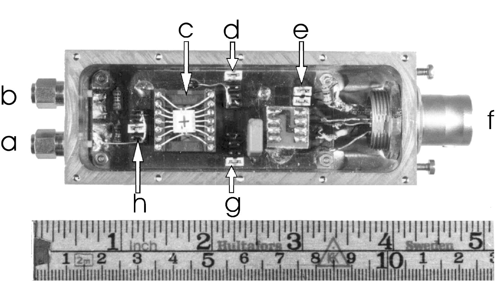
Fig. 2-2. The cold box, which is to be mounted in the cryostat. a) IN- input, b) IN+ input, c) MESFET chip, d) drain jumpers, e) test coax jumpers, f) LEMO connector (to dipstick), g) source jumpers and h) gate jumpers.
The dipstick is made of a thin walled stainless steel tube onto which brass sockets are soldered, one at each end of the tube. The sockets house the LEMO connectors. The length of the tube is 1 (one) m. The stick is mounted through a KF-50 flange to make a vacuum connection to the dewar. The stick is greased with vacuum grease and can then slide through the flange making it possible to set the box height relative the helium level. The coaxes used in the stick are 1 m of UT 20-SS, a semi-rigid coax with a center lead diameter of only 5 mils (0.13 mm). The material is stainless steel, chosen for its relatively poor heat conductivity. The DC lines are Teflon-insulated silver-coated wires of AWG 36 with a small diameter 0.40 mm to minimize heat leaks. The lines were twisted in pairs and these pairs were twisted in turn to minimize pick-up loop area.
The warm box contains the JFET, the three trimmers and the op-amp output stages as well as input/output connectors all housed in an aluminum shielded box. It is shown in Fig. 2-3 . Lines from the cryogenic stage enters the LEMO contact. The test input leads are separated directly and connected via a series resistor to a BNC connector mounted in the chassis. The series resistance was chosen rather arbitrarily to 12 kohm. The signal from the MESFET is fed to the JFET located at a small printed circuit board (PCB) just below the LEMO connector. The drain of the JFET is then fed through a small piece of coax to the main PCB were the signal is filtered and amplified and is finally output at two BNC connectors. The three bias lines are fed from the LEMO connector via the small PCB to the main PCB through a ribbon cable and ends up at the trimmers were biasing is adjusted. A good ground-plane is achieved on the main board in the same way as in the cold box.
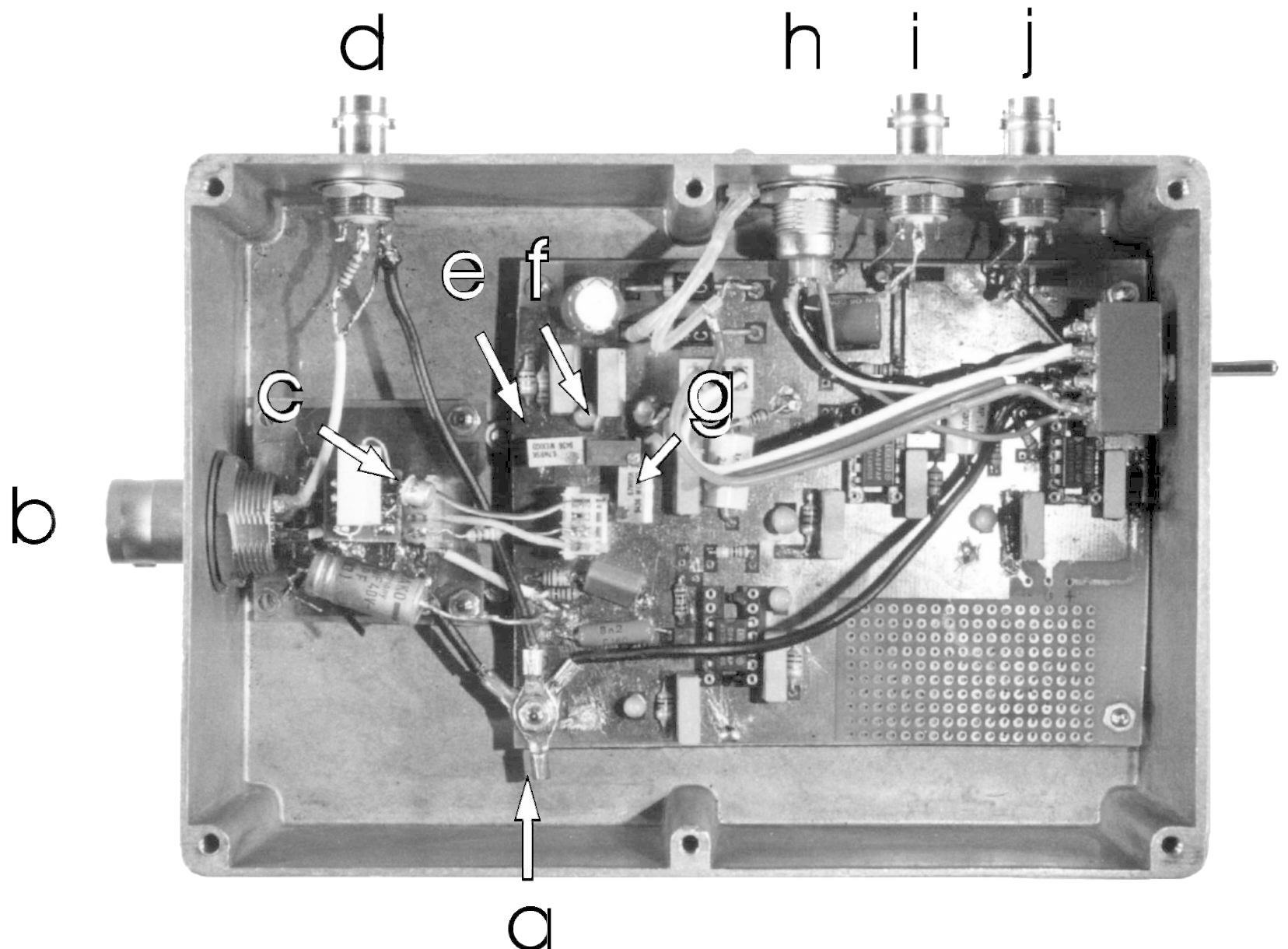
Fig. 2-3. The warm box. A small PCB to the left in the picture contains the upper part of the cascode. The larger PCB contains the op-amp stages, the trimmer resistors and power supply circuits. a) common ground point, b) LEMO connector (to dipstick), c) Si JFET, d) test input, e), f) and g) are gate, drain and source trimmers respectively, h) power supply input, i) x 250 output and j) x 2000 output.
2.4 Grounding Techniques
The circuit is designed using a single ground-point philosophy i.e. all subsystems' signal grounds should be connected in a tree-like fashion, branching from one common ground point without any loops. This ground point is shown in Fig. 2-3. Here the small PCB, test input and power ground meet at the same screw. The screw then connects to the main PCB by a nut and the screw head contacts the chassis to get a shielded box. The two outputs i) and j) which are isolated from the chassis, are not grounded this way but are instead connected directly to the top ground-plane of the main board.