Leonid Kuzmin - contact person
Associate Professor
Department of Microelectronics and Nanoscience
Physics and Engineering Physics
Chalmers University of Technology
S-41296 Gothenburg,
Sweden
Tel: +46 31 772 3608
Mobile: +46 73 909 31 55
Fax: +46 31 772 3471
e-mail: kuzmin@fy.chalmers.se
WWW: http://fy.chalmers.se/~kuzmin/
Tord Claeson,
Professor
Department of Microelectronics and Nanoscience
Physics and Engineering Physics
Chalmers University of Technology
S-41296 Gothenburg,
Sweden
Tel: +46 31 772 3304
Fax: +46 31 772 3471
e-mail: f4atc@fy.chalmers.se
Type of project: Subsystem
Summary
In the last decade superconducting detectors have become the most sensitive radiation detectors of Sub-mm, Infrared, and optical radiation with an estimated ultimate sensitivity down to 10-20 W/Hz1/2[1-3]. This sensitivity even allows for single photon counting with high detection efficiency and moderate (l /Dl= 5) to good (l /Dl= 1000) spectral resolution from the IR region to the X-ray range, respectively.
When developed into imaging arrays they will become the most sensitive imaging devices for astronomy. A few modest imaging arrays for ground-based sub-mm observations are already operational and plans for building significant larger arrays, SCUBA II, are approved. The coming decade will show the development of large (> 100 ´ 100 pixels) imaging arrays of superconducting detectors for all kinds of applications and for wavelengths from the Sub-mm to the X-ray range. This requires further developments of the various type of Superconducting detectors and further development of technological aspects like, development of detector arrays, superconducting electronics and multiplexing schemes for the read-out, low temperature (100 mK) cooler development and cryogenic wiring and packaging.
Europe has a large contribution in the development of this new area of Superconducting Detectors and Electronics and is in a favourable competitive position. A strong team of 17 groups from 11 countries has made a proposal for the ESF Network "Superconducting Detector Technology for Imaging Arrays". Chalmers Unversity (L. Kuzmin) is coordinator of this network [3],(Appendix1)
http://fy.chalmers.se/~kuzmin/Projects/ESF-SuperDet.html
We ask about corresponding national support for development of imaging arrays in mm/submm region and their applications for astronomy projects. We have preliminary agreement about participation with imaging arrays of bolometers in ELISA balloon borne experiment led by CNRS, Toulouse. The developed arrays of bolometers can be used for other submillimeter telescopes: observatory Testa Gridgia (Italy, Roma University), SEST telescope (Swedish submillimeter telescope in Chili), ALMA single dish telescope (MPIfR-Bonn project of submillimeter telescope, in Chili) Grenoble observatory (France), IRAM, Archeops balloon telescope (CRBT/Grenoble, IAS/Paris), Pronaos telescope (CNRS, Toulouse, France), and space telescope Submillimetron..
Status of relevant research, objectives and execution plan
Superconductive radiation sensors are nowadays available from the Sub-mm to the X-ray range [1-3]. One can distinguish roughly two types: power sensors from mm to IR range with extremely low Noise Equivalent Power (NEP) down to 10-20W/Hz1/2 and single photon counters from IR to X-ray range. The power sensors successfully developed sofar are bolometers with either phase-transition thermometers (superconductor to normal conductor), called Transition Edge Sensors (TES) [4-6] ] or normal metal hot-electron bolometers (NHEB) with Superconductor-Isolator-Normal metal (SIN) junction thermometers [7-9]. The main efforts at Chalmers University are directed to antenna coupled version of the NHEB. Normal metal Hot-Electron nanoBolometers (NHEB) [9,10] has shown record level of sensitivity NEP = 3x10-18 W/Hz1/2 in dc measurements. Original type of cryogenic submillimeter bolometer with tunnel junctions for capacitive coupling and thermal protection has been successfully developed for this project at Chalmers University (Fig. 1a) [11]. The programme of bolometer development is described in the Roadmap [12]. Optical measurements are made in 3He cryostat at 300 mK fabricated by CEA, Grenoble. The methodics of quasioptical qualification is developed in cooperation with group of Paul Richards, Berkeley [13].
The exciting effect of nonequilibrium electron cooling has been demonstrated by Nahum et al., [14] for normal metal strip connected to SIN tunnel junctions. The results of Jyväskylä group [15] on electron cooling from 300 mK to 120 mK attract interest from ESA. The group is working now on electron cooling of substrate for submm and x-ray sensors under contract with ESA. We cooperate with this group for selection the best configuration of the bolometer. A novel concept of "cold-electron" bolometer with direct electron cooling of absorber has been proposed by Kuzmin et al. [16]. This bolometer can be especially effective for operation in presence of a realistic background power load. The optimal configuration of this sensor is a hot-electron bolometer with capacitive coupling to the antenna by tunnel junctions [11] developed at Chalmers University (Fig. 1).
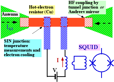
Figure 1. a) Schematics of the NHEB bolometer with SIN (superconductor-insulator-normal metal) thermometers and a SQUID readout system. S - superconductive layer, N - normal metal layers, V ó voltage bias, X - SQUID tunnel junctions. B) AFM picture of bolometer with tunnel junctions for high frequency coupling and thermal isolation of the absorber.
An intensive development of imaging arrays of superconducting sensors for submm, IR and X-ray wavelength together with associated cryogenic cooling and cryopackaging is made for ground-based and space-based astronomy [1-4]. Intensive works on development of imaging arrays of bolometers with the SQUID readout system (Fig. 1b) are conducted in NIST and NASA/Goddard (SPIRE: 64x64 array - goal, 1x8 array - tested; Constellation-X: arrays up to 100x100 - goal). The SQUID readout systems for X-ray (XEUS: arrays from 32x32 to 100x100 -goal) and IR arrays are under development by ESA subcontractors. The Submillimetron Project for the ISS requires array of sensors from 10x10 to 32x32 pixels [17]. The imaging arrays developments are extremely important for applications. These developments involve sensor production aspects, development of multiplexing schemes to read-out large detector arrays with particular emphasis on superconducting electronics, sensor packaging and wiring, and 100 and 300 mK cooler developments. These aspects, mainly technological, are in the stage of intensive development. Adiabatic Demagnetization Refrigerators [ADR] are becoming commercially available with enough cooling power and low enough temperatures (50 mK) for sensor arrays.
The great advantage of SQUID sensor is full technological, material and temperature compatibility with superconducting bolometers arrays. SQUID operates much better at millikelvin temperatures compared to higher temperatures in contrast to any semiconducting amplifier that in principle cannot work at mK. SQUID has extremely low power dissipation that makes it most attractive to read out the arrays with amount of pixels over 100. Integrating the SQUID with bolometer greatly reduce the length of wiring and pickup area for external noise. No other type of amplifier can bring such possibilities. For 32x32 array a SQUID multiplexed readout needs 100 wires instead of 2000 with a plain expansion of existing arrays [3,4].
The analysis shows that SQUID current sensitivity of a level of 10-50 fA/Hz1/2 is necessary for realization of high sensitivity of NHEB [18]. Such improvement of SQUID sensitivity can be realized by using cryogenic transformer. The works on SQUID readout system for imaging arrays have already started at Chalmers University in cooperation with VTT, Finland and several other countries, supported by the INTAS foundation [19]. SQUID femtoamperemeter with ferromagnetic transformer has shown current sensitivity better than 30 fA/Hz1/2 at 4.2 K [19]. This level of current noise will allow to realize a high sensitivity of microbolometers with NEP = 10-18 W/Hz1/2 required for applications. Our goal is to improve further sensitivity and increase the number of addresses of SQUID multiplexer [20].
Taking into account that development of this vast region demands wide international contacts and new young forces, the Chalmers group has organized several International Workshops and Schools for young scientists on this topic [21].
Objectives of the proposal are:
Design and test of different concepts of hot-electron bolometers at wavelength from 1 mm to 150 mm at 100 and 300 mK using technological facilities of Chalmers University. (2002-2004)
Fabrication of small scale array of bolometers with eight pixels in a cryostat with double stage 3He cooler at T = 200-300 mK. CEA (Lionel Duband) and Air Liquide (Alain Ravex), Grenoble, show interest to participate in this programme with their advanced cryocooler. The SQUID readout system will be developed in cooperation with VTT (Heikki Seppa), Finland. (2002-2003)
Design, fabrication and testing of a fly prototype arrays of bolometers for the ELISA balloon borne experiment (300 mK focal plane) (in collaboration with CNRS (Martin Giard), Toulouse). ELISA is devoted to sensitive surveys of the Galaxy ±30 degrees at 170, 240, 400 and 650 microns (3.5 arcmin beam) (2002-2004)
Development of large scale arrays from 10x10 to 32x32 pixels; (2003-2005)
Development of multiplexing SQUID readout system for large scale arrays more than 100 pixels
Participation in other European projects of submillimeter telescopes (should be discussed)
European context:
All works will be made in tight cooperation with participants of the ESF Network "Superconducting detector technology for imaging arrays" [3], (Appendix 1).
The European Network of Excellence on Superconductivity (SCENET) monitors the applications of superconductivity. A special interest to superconducting detectors and bolometers is shown in the Network activity (see the Roadmap [2]). ESF Network is directly connected to the SCENET.
Technological facilities and Group experience
The Chalmers Univesrity has got world class technological and experimental facilities in a new Microtechnology Center -MC2 [22] as well as experienced personnel capable to accomplish the tasks of the project. The proposal is based on extensive preliminary investigations carried out over the last years in the field of superconducting detectors and possible applications. The project group based at Chalmers University with wide international collaboration has many years of successful experience in studies of ultimate parameters of superconducting devices, including mixers, detectors, spectrometers, RF amplifiers. The group has gained experience in studies of noise in superconducting devices, in fabrication of ultra-low-noise SIS and Josephson receivers, Hilbert spectrometers, SQUID magnetometers and amplifiers, InSb bolometers as well as NHEB elements. The technological facilities and reliable procedures for fabrication of nanoscale Al-based and Nb-based tunnel junctions have already been developed. Such junctions are used in bolometer structures and in SQUID readout systems intended for femtoampermeter readout of NHEB bolometer. The Chalmers group has good experience in Single Electronics and nanofabrication. The results in single-electron tunneling gained by the group together with their facilities in fabrication of submicrometer size structures and facilities for measurements in the millikelvin temperature range, bring a possibility to fabricate and develop the novel ultra-sensitive structures with submicrometer dimensions. The group from Chalmers has many years of experience and unique facilities for measurements of signal and noise parameters in superconducting submm-wave detectors. The experience and the proposed new ideas in methods of optimal matching of superconducting devices bring possibilities to optimize the front-end of the detectors. The NHEB samples using Al based junctions have shown high sensitivity better than 3*10-18 W/Hz1/2 and proved compatibility with available technology at Chalmers. The non-equilibrium effects in superconducting structures give a possibility to fabricate a novel hot-electron bolometer with an estimated noise equivalent power of the order of 10-18 W in a 1 Hz bandwidth that is one order of magnitude better than existing semiconductor bolometers. Another important component is RF and submm-wave technique and experience in design and studies of microwave characteristics in superconducting devices. Such facilities, equipment and experience are gained in involved research teams, in different spectral regions, and uniting them in joint project allows to develop and to study microwave devices in a wide frequency range.
Expected benefits
REFERENCES
Appendix 1
Collaboration with European research groups in scope of the ESF
Network "Superconducting Detector Technology for Imaging Arrays":
2. Germany, Institute of Space Sensor technology and Planetary Exploration , Berlin (Heinz-Wilhelm Hubers - applicant, Alexei Semenov). Superconducting Quantum detectors;
IPTH Jena, (Hans-Georg Meyer), SQUID readout systems
3. Netherlands. SRON, Utrecht (Piet de Korte - applicant), Imaging arrays of TES-based X-ray spectrometers for XEUS
4. United Kingdom. Leicester University, Astro Space Center (Andrew Holland), Imaging X-ray detectors based on TES technology;
UKATC, Royal Observatory (William Duncan), Bolometer arrays for SCUBA
5. Finland. University of Jyvaskyla, (Jukka Pekola); TES sensors
for IR and X-ray;
Metorex, (Heikki Sipilä), TES sensors for IR and X-ray;
VTT, Helsinki (Heikki Seppa), SQUID readout system based on frequency domain multiplexing.
6. Italy, CNR-Instituto di Cibernetica, Naples (Roberto Christiano), STJ-detectors for X-ray imaging
7. France, CEA, Grenoble (Lionel Duband), Cryorefrigerators ;
AIR LIQUIDE, Grenoble (Alain Ravex), Cryorefrigerators ;
CNRS, Toulouse (Martin Giard). Bolometer arrays for balloon experiments
8. Denmark, DTU, Lyngby, (Jesper Mygind), Cryogenic measurements of superconducting detectors
9. Norway, Oslo University, (Dragos-Victor Anghel Department of Physics. Theory of sensors with SIN tunnel junctions
10. Estonia, Institute of Physics, Tartu, Ants Löhmus, Cryorefrigerator
11. Switzerland, Paul Scherrer Institute, VILLIGEN, (Philippe Lerch). Imaging arrays of STJ based X-ray spectrometers.