MAKING GOLD PADS
-
On the
spinner, rinse silicon dioxide wafer with acetone and isopropanol.
-
Spin LOL2000
@ 3000 rpm (3s acceleration and deceleration).
This gives about
200 nm thickness of the undercut layer according to the figure below.
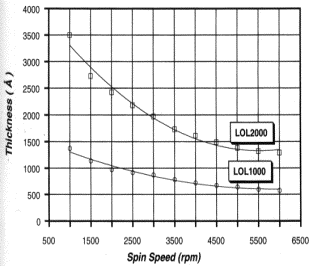
Picture
taken from the SNL webpage.
http://fy.chalmers.se/assp/snl/
-
Bake the
sample @ 180
°C for 10
mins.
-
Spin Shipley
UV5Ô DUV photoresist
@ 4000 rpm (3s acceleration and deceleration).
This
gives about 630 nm thickness of the top photoresist layer according to the
figure below.
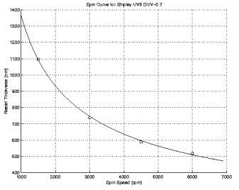
Picture taken
from the SNL webpage.
http://fy.chalmers.se/assp/snl/
-
Bake the
sample @ 130
°C for 1 min
and 30 secs.
-
Expose on
Mask Aligner KS-MJB3 DUV for 7-8 seconds.
By default, the intensity is
set at 1.6 mJ/cm2. Keep in mind that the product of the intensity
(measured using the intensity meter) and the exposure time should be equal to
the energy per unit area, which is 3.8 mJ/cm2.
-
Bake the
sample @100
°C for 1 min.
-
Develop
using MF319.
An
indication when it is ready would be when the color in the region of the pattern
changes plus about 10-15 secs.
-
Rinse in DI
water thoroughly, and blow dry carefully.
-
Check in the
optical microscope if the pattern is acceptable.
-
Ash at 50 W,
250 mTorr oxygen for 30 secs.
-
Evaporate
the contact pads.
Cr is
used for good adhesion between silicon and gold. A thin layer of Cr would
suffice. Then Au is evaporated. Finally, Pd is added for protection. When Al is
evaporated on top of gold, Au-Al intermetallic bonds may be formed across the
contact area, which increases the contact resistance. This is undesirable for
our purposes. Intermetallic compounds have differing structures, crystal
lattice constants and volume expansion coefficients. These differences form
cracks along the intermetallic phase boundary stress surfaces. To avoid these faults,
an intermediate metal is formed to prevent physical contact between Au and Al.
-
Spin Shipley
S1813 photoresist @4000 rpm for 2-5 minutes.
The purpose of the photoresist in this case is to protect
the sample from getting dirty during wafer cutting. So the parameters are not
really important.
-
Bake sample
@ 100
°C for 2
minutes.
-
Cut wafer.
-
Remove
photoresist in Microposit Remover 1165 bath.
It may
be good to have an extra beaker with remover or acetone to remove residual
photoresist.
-
Rinse
thoroughly in isopropanol bath, and blow dry carefully.
-
Check in the
optical microscope if the pattern is acceptable.