In order to extract top performance out of a computer system, it is important to understand the architecture of the system. In this section, we describe the architecture of the Origin2000 system and the components which comprise it, including the R10000 microprocessor.
The Origin2000 is a Scalable Shared Memory Multiprocessor (S2MP). In this section, we will describe what this phrase means and why the Origin2000 uses this new architecture.
Since there is always a limit to the performance of a single processor, computer manufacturers have increased the performance of their systems by incorporating multiple processors. Two approaches for utilizing multiple processors have emerged: shared memory implementations and distributed memory implementations.
Previous shared memory computers, including Silicon Graphics's Power Series, Challenge and Power Challenge systems, utilize a bus-based architecture. In this architecture, processor and memory boards plug into a common bus; communication between the hardware components occurs on the bus.
This architecture has many desireable properties. Each processor has direct access to all the memory in the system. This allows efficient multitasking and multiuser use of the system through symmetric multiprocessing. In addition, parallel programs are relatively easy to implement on these types of systems. Parallelism may be achieved by simply inserting directives into the code to distribute the iterations of loops among the processors. An example of this is shown below:
c$doacross local(j,i), shared(n,a,r,s), mp_schedtype=simple
      do j = 1, n
         do k = 1, n
            do i = 1, n
               a(i,j) = a(i,j) + r(i,k)*s(k,j)
            enddo
         enddo
      enddo
Here, the simple schedule type means that blocks of consecutive iterations are assigned to each processor. That is, if there are p processors, the first processor is responsible for executing the first ceil(n/p) iterations, the second processor executes the next ceil(n/p) iterations, and so on.
Loops without parallelization directives run sequentially.
One of the advantages of this shared memory parallelization style is that it can be done incrementally. That is, the user can identify the most time consuming loop in the program and parallelize just it. The program can then be run to validate correctness and measure performance. If a sufficient speedup has been achieved, the parallelization is complete. If not, additional loops can be parallelized one at a time.
Another advantage of the shared memory parallelization is that loops can be parallelized without concern for which processors have accessed data elements in other loops. In the parallelized loop above, the first processor is responsible for updating the first ceil(n/p) columns of the array a. In the loop below, an interleave schedule type is used which means that the first processor will access every p-th column of a (different schedule types are used to more evenly distrubute work among the processors):
c$doacross local(kb,k,t), shared(n,a,b), mp_schedtype=interleave
      do kb = 1, n
         k = n + 1 - kb
         b(k) = b(k)/a(k,k)
         t = -b(k)
         call daxpy(k-1,t,a(1,k),1,b(1),1)
      enddo
Since all data are equally accessible by all processors, nothing special needs to be done for a processor to access data which were last touched by another processor; each processor simply references the data it requires. This makes parallelization easier since the programmer only needs to expend effort making sure the processors have an equal amount of work to do; it doesn't matter which subset of the work a particular processor does.
Let's now contrast the shared memory approach with the distributed memory approach. In a distributed memory computer, there is no common bus to which memory attaches. Each processor has its own local memory which only it can access directly. In order for a processor to have access to the local memory of another processor, a copy of the desired data elements must be sent from one processor to the other. Typically, this data communication, called message passing, is accomplished using a software library. MPI and PVM are two commonly used message passing libraries.
In order to run a program on a message passing machine, it is responsibility of the programmer to decide how the data are to be distributed among the local memories. All data structures which are to be operated on in parallel must be distributed. In this approach, incremental parallelism is not possible. The key loops in a program will typically reference many data structures; each must be distributed in order to run that loop in parallel. And once a data structure has been distributed, all sections of code which reference it must be run in parallel. The result is an "all or nothing" approach to parallelism on distributed mmeory machines. In addition, note that since many programs's data structures are bigger than a single local memory, it may not even be possible to run the program on the machine without first parallelizing it.
In the shared memory section above, we saw that different loops of a program may to be parallelized in different ways to ensure an even allocation of work among the processors. On a distributed memory machine, this translates into data structures needing to be distributed differently in different sections of the program. Redistribution of the data structures is the responsibility of the programmer, who must find efficient ways to accomplish the needed data shuffling. Such issues never arise in the shared memory implementation.
The bottom line is that programming is much easier on a shared memory computer.
So why then would anyone build anything but a shared memory computer? The reason is scalability. Below is a table showing the performance of the NAS Parallel Benchmark kernel FT running on a Power Challenge 10000 system. Results are presented for a range of processor counts and two problems sizes: ClassA represents a small problem size, and the ClassB problem is four times larger. What we see from these results is that the performance scales well up through 8 processors, but then it levels off; the 16-processor times are only slightly better than the 12-processor times.
nprocs   ClassA  SpeedUp  Amdahl    ClassB  Speedup  Amdahl
   1      62.73    1.00    1.00     877.74    1.00    1.00
   2      32.25    1.95    1.95     442.66    1.98    1.98
   4      16.79    3.74    3.69     225.10    3.90    3.90
   8       9.58    6.55    6.68     125.71    6.98    7.54
  12       7.96    7.88    9.16     103.44    8.49   10.96
  16       7.55    8.31   11.24      98.92    8.87   14.16
The reason for this leveling off is the bus in the shared memory system. The bus is limited to a finite bandwidth and a finite number of transcations that it can carry out per second. With high performance microprocessors such as the R10000, the demands placed on the bus by a single processor are large enough that the bus's capacity can be exhausted. For this particular program, the limit has been reached when 12 processors are used simultaneously; for other programs, the number of processors needed to reach this limit will vary. But once this limit has been reached, utilizing more processors will not significantly increase a program's performance.
Note that one should not assume that these programs would be capable of achieving perfect speedup were it not for the limits imposed by the bus. We can make an estimate of how much performance is lost due to bus saturation using Amdahl's Law. This rule of parallel computation states that the performance gain one may achieve from parallelizing a program is limited by the amount of the program which runs sequentially. More specifically, if s is the portion of a program which runs sequentially, and p is the part which runs in parallel (s + p = 1), the parallel speedup is
             s + p           1           1
SpeedUp  =  -------  =  -----------  <=  -
            s + p/n     s + (1-s)/n      s
Using this formula and the results above for 2 processors, we can estimate the portions of the ClassA and ClassB problems which are run sequentially:
                             1
FT Class A: 1.9451   =  -----------  ->  s = 0.02822, p = 0.97178
                        s + (1-s)/2

                             1
FT Class B: 1.98288  =  -----------  ->  s = 0.00863, p = 0.99137
                        s + (1-s)/2
With these values for s, the Amdahl's Law limits on speedup for any number of processors can be calculated from the above formula; these results are given in the table under the columns labeled Amdahl. These are the speedups one would expect to achieve with no bus saturation; they indicate the performance that could be achieved on a distributed memory machine whose per-processor performance is exactly the same as the Power Challenge 10000.
So, while a bus-based shared memory machine offers a familiar multi-tasking, multi-user environment and relative ease in parallel programming, the finite bandwidth of the bus can become a bottleneck and limit scalability. Distributed memory message-passing machines cure the scalability problem by eliminating the bus, but thrown out with the bus is the shared memory model and the ease of programming it allows. Ideally, what we would like is one machine which combines the best of both approaches. This is what the scalable shared memory of the Origin2000 provides.
The Origin2000 uses physically distributed memory; there is no longer a common bus to become a bottleneck. Memory bandwidth grows as processors and memory are added to the system, but the Origin2000 hardware treats the memory as a unified, global address space, so it is shared memory just as on a bus-based system. The programming ease is preserved, but the performance is scalable.
The improvement in scalability is easily observed in practice. Below is a table showing the performance of the the NAS Parallel Benchmark kernel FT on an Origin2000 system:
nprocs   ClassA  SpeedUp    ClassB  Speedup
   1      55.43    1.00     810.41    1.00
   2      29.53    1.88     419.72    1.93
   4      15.56    3.56     215.95    3.75
   8       8.05    6.89     108.42    7.47
  16       4.55   12.18      54.88   14.77
  32       3.16   17.54      28.66   28.28
We can see that programs with sufficient parallelism now scale to as many processors as are available. And what's more, this is achieved with the same code as was used on the bus-based shared memory system.
In addition, you may have noticed that the per-processor performance on Origin2000 is better than on Power Challenge 10000. This is due to the improved memory access times of the Origin system. This is but one of the many details we will explore as we describe the architecture of the Origin2000 system in the next several sections.
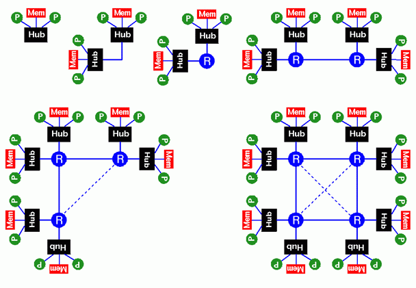
In order to understand how the Origin2000's Scalable Shared Memory Multi-Processor (S2MP) architecture works, we first look at how the building blocks of an Origin system are connected. This is diagrammed in the figure below.
Here we see diagrams of Origin systems ranging from 2 to 16 processors. We start by considering the 2-processor system in the upper left corner of the figure. This is a single Origin2000 node. It consists of 1 or 2 processors, memory, and a device called the hub. The hub is the piece of hardware that carries out the duties that a bus performs in a bus-based system; namely, it manages each processor's access to memory and I/O. This applies to accesses which are local to the node containing the processor, as well as to those which must be satisfied remotely in multi-node systems.
The smallest Origin systems consist of a single node. Larger systems are built by connecting together multiple nodes. A two-node system is shown in the upper middle of the figure. Since information flow in and out of a node is controlled by the hub, connecting two nodes means connecting their hubs. In a two-node system this is simply a matter of wiring the two hubs together. The bandwidth to local memory in a two-node system is double that in a one-node system: the hub on each of the two nodes can access its local memory independently of the other. Access to memory on the remote node is a bit more costly than to the local memory since the request must be handled by both hubs. A hub determines whether a memory request is local or remote based on the physical address of the datum accessed.
When there are more than two nodes in a system, their hubs cannot simply be wired together. In this case, additional hardware is required to control information flow between the multiple hubs. The hardware used for this in Origin systems is called a router. A router has six ports, so it may be connected to up to six hubs or other routers. In a two-node system, one may employ a router to connect the two hubs rather than wiring them directly together; this is shown adjacent to the other two-node configuration in the figure. These two different configurations behave identically, but due to the presence of the router in the second configuration, information flow between the two hubs takes a small additional amount of time. The advantage, though, of the configuration with the router is that it may then be used as a basic building block from which to construct larger systems.
In the upper right corner of the figure, a 4-node --- or, equivalently, 8-processor --- system is shown. It is constructed from two of the two-node-with-router building blocks. Here, the connection between the two routers allows information to flow, and, hence, the sharing of memory, between any pair of hubs in the system. Since a router has 6 ports, it is possible to connect all 4 nodes to just one router, and this one-router configuration can be used for small systems. However, that is a special case, and the two-router implementation is used in general since it conveniently scales to larger systems.
Two such larger systems are shown on the lower half of the figure; these are 12- and 16-processor systems, respectively. From these diagrams you can start to see how the router configurations scale: each router is connected to 2 hubs, then routers are connected to each other forming a binary n-cube, or hypercube, where n, the dimensionality of the router configuration, is the base-2 logarithm of the number of routers. For the 4-processor system, n is 0, and for the 8-processor system, the routers form a linear configuration, and n is 1. In both the 12- and 16-processor systems, n is 2 and the routers form a square; for the 12-processor system, one corner of the square is missing. Larger systems are constructed by increasing the dimensionality of the router configuration and adding up to two hubs with each additional router. Systems with any number of nodes may be constructed by leaving off some corners of the n-dimensional hypercube. We will see these larger configurations later.
The key thing to note here is that the hardware allows the physically distributed memory of the system to be shared just as in a bus-based system, but since each hub is connected to its own local memory, memory bandwidth is proportional to the number of nodes. As a result, there is no inherent limit to the number of processors that can be used effectively in the system. In addition, since the dimensionality of the router configuration grows as the systems get larger, the total router bandwidth also grows with system size (proportional to n2n, where n is the dimensionality of the router configuration). Thus, systems may be scaled without fear that the router connections will become a bottleneck.
However, to allow this scalability, one nice characteristic of the bus-based shared memory systems has been sacrificed. Namely, the access time to memory is no longer uniform: it varies depending on how far away in the system the memory being accessed is. The two processors in each node have very quick access through their hub to their local memory. Accessing remote memory through an additional hub adds an extra increment of time, as does each router the data must travel through. But several factors combine to smooth out these non-uniform memory access (NUMA) times.
Thus, the architecture of the Origin2000 system provides shared memory hardware without the limitations of traditional bus-based designs. Let's now look in more detail at the components that comprise the system.
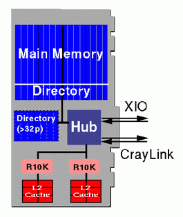
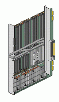
An Origin system starts with a node board. Below, on the left, is a schematic of an Origin2000 node board; a drawing of the node board is shown on the right:
Each node contains 1 or 2 R10000 processors. A description of the R10000 processor will be given later. In Origin2000 systems, node boards are available in two configurations:
All node boards in a system must be of the same configuration.
Each processor and its secondary cache is packaged into a subassembly called a Horizontal Inline Memory Module (HIMM). Two HIMMs are shown at the bottom of the above node board drawing. In general, each node board comes with two processors installed, but it is possible to start a 180 MHz system with just one processor on the first node board; after that, all node boards will come with two processors. On 195 MHz systems, all node boards have two processors installed.
In addition to the processors, the node board has 16 sockets to hold memory. Memory modules are installed in pairs, so they are given the name Dual Inline Memory Modules (DIMMs). Each DIMM-pair represents one bank of memory. Eight main memory DIMM-pairs may be installed in a node board. These DIMM-pairs come in three sizes:
At least one pair of DIMMs must be installed, so a node board may be configured with 64 MB to 4 GB of memory.
In order to sustain high bandwidth, memory systems are interleaved on cache line addresses; sequential accesses to different leaves allow the full bandwidth of the memory system to be sustained. Each DIMM-pair in an Origin2000 node board provides 4-way memory interleaving. The memory subsystem is fast enough that 4-way interleaving can provide full memory bandwidth, so it is not necessary to populate more than one bank in order to achieve top performance. (Note that this differs from Power Challenge systems in which using multiple memory boards in order to achieve 4- or 8-way memory interleaving is recommended for the best memory performance on large configurations.)
In addition to memory provided by the specified size, each main memory DIMM contains extra memory. Part of this is used to provide single-bit error correction, dual-bit error detection. The rest stores what is known as a directory. Since there is no common bus in the Origin system, a mechanism different than what is used in bus-based shared memory machines is required to keep information stored in the processor caches coherent; the scheme used in Origin is called directory-based cache coherence. This will be described in more detail in the following section. But what it means for the memory in the system is that the main memory DIMMs must store an additional amount of information whose size is proportional to the number of nodes in the system.
Since Origin systems can scale to quite a large number of nodes, a significant amount of directory information would be required in each main memory DIMM to allow systems to be built to the largest configuration. In order to not have to burden smaller systems with wasted directory memory, the main memory DIMMs provide only enough directory storage for systems with up to 16 nodes (i.e., 32 processors). For larger systems, additional directory memory is installed in separate directory DIMMs. Sockets for these DIMMS are provided below the main memory DIMMs as can be seen on the above schematic. In systems with 32 or fewer processors, the directory overhead amounts to less than 6% of the storage on a DIMM; for larger systems, it is less than 15%. This is comparable to the overhead required for the error correction bits.
The final component of the node board is the hub. As we saw in the previous section, the hub controls the processors's access to memory and I/O. The hub has a direct connection, called the SysAD bus, to the main memory on its node board. This connection provides a raw memory bandwidth of 780 MB/s (720 MB/s in a 180 MHz configuration) for the two R10000s on the node board to share. In practice, however, data cannot be transferred on every bus cycle, so achievable bandwidth is more like 600 MB/s.
Access to remote memory is through a separate connection called the CrayLink interconnect. This bidirectional interconnect attaches to either a router or another hub. It is bidirectional and has a raw bandwidth of 780 MB/s in each direction (720 MB/s in a 180 MHz configuration).The effective bandwidth a user program will achieve is less than this, about 600 MB/s in each direction, since not all information sent through the CrayLink is user data.To request a copy of a cache line from a remote memory, a hub must first send a 16-byte address packet to the hub attached to the remote memory; this specifies which cache line is desired and where it needs to be sent. Then, when the data are returned, along with the 128-byte cache line of user data, another 16-byte address header is sent (so the receiving hub can discern this cache line from others it may have requested). Thus, 16+128+16 = 160 bytes of data are passed through the CrayLink interconnect to transfer the 128-byte cache line, so the effective bandwidth is 780 * (128/160) = 624 MB/s in each direction (576 MB/s in each direction for the 180 MHz configuration).
The hub also controls access to I/O devices. This is through a channel called XIO. Electrically, this connection is the same as the CrayLink, but different protocols are used in communicating data. The bandwidth is the same as CrayLink. Routers allow multiple hubs to be connected to each other in order to communicate via CrayLink. Shortly, we'll describe the analogous hardware device which permits a hub to be connected to multiple I/O devices using XIO.
Each CPU in an Origin system has a private cache memory of 1 MB or 4 MB. In order to get good performance, the CPU always fetches and stores data in its cache. When the CPU refers to memory that is not present in the cache, there is a delay while a copy of the data is fetched from memory into the cache. The CPU's use of cache memory, and its importance to good performance, is covered in another topic.
The point here is this: there can be as many independent copies of a memory location as there are CPUs in the system. If every CPU refers to the same memory address, every CPU's cache will have a copy of that address. (This could be the case with certain kernel data structures, for example.) But what if one CPU then modifies that location? All the other cached copies of the location have become invalid. The other CPUs must be prevented from using what is now "stale data." This is the issue of cache coherence -- how to ensure that all caches reflect the true state of memory.
Cache coherence is not the responsibility of software (except for kernel device drivers, which must take explicit steps to keep I/O buffers coherent). In order for performance to be acceptable while maintaining the image of a single shared memory, cache coherence must be managed in hardware. Cache coherence is also not the responsibility of the R10000 CPU. Cache management is performed by auxiliary circuits that are part of the Hub chip discussed earlier.
The cache coherence solution in the Origin is fundamentally different from that used in the earlier Power Challenge systems. Because it has a central bus, the Power Challenge can use a "snoopy" system, in which each CPU observes every memory access that moves on the bus. When a CPU observes another CPU modifying memory, the first CPU can automatically invalidate and discard its now-stale copy of the changed data.
The Origin has no central bus, and there is no way for a CPU in one node to know when a CPU in a different node modifies its own memory, or memory in yet a third node. Origin systems could mimic what is done in bus-based systems; that is, all memory accesses could be broadcast to all nodes so that stale cache lines could be invalidated. But since all nodes would need to broadcast their memory accesses, this coherency traffic would grow as the square of the number of nodes. As more nodes are added to the system, all the available internode bandwidth would eventually be consumed by this traffic. As a result, the system would suffer from limitations similar to bus-based computers: it would not be scalable. So to permit the system to scale to large numbers of processors, a different approach to maintaining cache coherency is used. The Origin uses what is called a directory-based cache coherency scheme.
Briefly, here's how a directory-based cache works. (For a theoretical discussion of directory-based caches, see Lenoski, Daniel and Weber, Wolf-Dietrich, Scalable Shared-Memory Multiprocessing, San Francisco: Morgan Kauffman, 1995. For a detailed description of the Origin implementation of the Hub, see the Origin and Onyx2 Programmer's Reference Manual. )
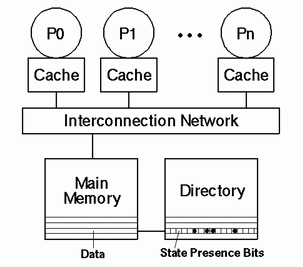
Memory is organized by cache lines of 128 bytes. Associated with the data bits in each cache line is an extra set of bits, the state presence bits -- one bit per node (in very large systems, those with more than 128 processors, one state presence bit represents more than one node, but the principle is the same), and a single number, the number of a node that owns the line exclusively. Whenever a node requests a cache line, its hub initiates the memory fetch of the whole line from the node that contains that line. When the cache line is not owned exclusively, the line is fetched and the state presence bit for the calling node is set to 1. As many bits can be set as there are nodes in the system.
When a CPU wants to modify a cache line, it must gain exclusive ownership. To do so, the hub retrieves the state presence bits for the target line and sends an invalidation event to each node that has made a copy of the line. Typically, invalidations need to be sent to only a small number of other nodes; thus, the coherency traffic only grows proportionally to the number of nodes, and there is sufficient bandwidth to allow the system to scale. Both CPUs on each of the nodes sent an invalidation request discard their cached copy of the line. The number of the updating node is set in the directory data for that line as the exclusive owner. When a CPU no longer needs a cache line (for example, when it wants to reuse the cache space for other data), the hub gives up exclusive access if it has it, and turns off its state presence bit.
When a CPU wants to read a cache line and the line is exclusively owned, the hub requests a copy of the line from the owning node. This retrieves the latest copy without waiting for it to be written back to memory. There are other protocols by which CPUs can exchange exclusive control of a line when both are trying to update it; and other protocols that allow kernel software to invalidate all cached copies of a range of addresses.
The directory-based cache coherency mechanism uses a lot of dedicated circuitry in the hub to ensure that many CPUs can use the same memory, without race conditions, at high bandwidth. As long as memory reads far exceed memory writes (the normal situation), there is no performance cost for maintaining coherence.
However, when two or more CPUs update the same cache line, alternately and repeatedly, performance suffers because every time either CPU refers to that memory, a copy of the cache line must be obtained from the other CPU. When the two (or more) CPUs are actually trying to update the same variables, you have memory contention. When the CPUs are updating distinct variables that only coincidentally occupy the same cache line, you have false sharing -- memory contention that arises by coincidence, not design.
Part of performance tuning of parallel programs is recognizing memory contention and false sharing, and eliminating it.
As mentioned above, the hub controls access to I/O devices as well as memory. Each hub has one XIO port. In order to allow connections to multiple I/O devices, each hub is connected to a Crossbow (XBOW) I/O controller chip. Up to two hubs may be connected to the same XBOW.
The XBOW is a dynamic crossbar switch which allows up to two hubs to connect to up to 6 I/O devices, as shown in the following diagram:
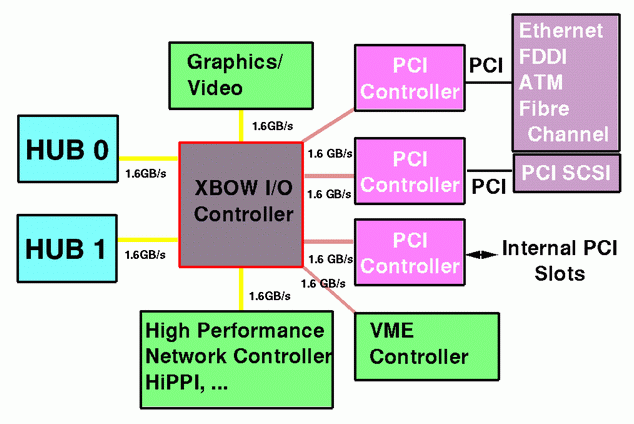
Each XIO connection, from hub to XBOW and from XBOW to I/O device, is bi-directional with a raw bandwidth of 780 MB/s in each direction (720 MB/s for 180 MHz configurations). Like the CrayLink interconnect, some of the bandwidth is used by control information, so achievable bandwidth is approximately 600 MB/s in each direction.
XIO connections to I/O devices are 16 bits wide, although an 8-bit subset may be used for devices for which half the XIO bandwidth is sufficient. Currently, only SGI graphics devices utilize the full 16-bit connection. Industry standard I/O interfaces such as ethernet, FDDI, ATM, Fibre Channel, HiPPI, SCSI and PCI operate at more modest bandwidths, so XIO cards supporting these devices employ the 8-bit subset. Each standard interface card first converts the 8-bit XIO subset to the PCI bus using a custom chip called the PCI adaptor, and then readily available hardware is employed to convert the PCI bus to the desired standard interface.
One particular standard interface card, the IO6, must be installed in every Origin2000 system. This IO card supplies two SCSI buses to provide the minimal I/O requirements of a system; namely, it allows the connection of a CD-ROM drive, for loading system software, and a system disk. It also contains serial and ethernet and ports to allow attachment of a console and external network.
If two nodes are connected to a XBOW, control of the 6 I/O devices is statically partitioned between the two nodes at system boot time. If one of the nodes is inoperable, the second can be programmed to take control of all of them. Note, though, that Origin is a shared memory system, so all processors in the system can access any I/O device, either directly through a XBOW or via a request to another hub.
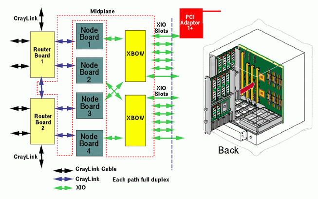
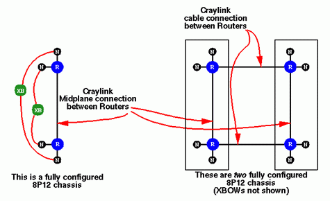
In Origin2000 systems, XBOWs are located on the midplane of an Origin module, shown above. There are two XBOWs in each module, thus providing connections for up to 12 XIO cards and 4 node boards. The I/O devices attached to a XBOW can only be active if the XBOW is attached to at least one node, so connections from node boards to XBOWs are interleaved. That is, nodes 1 and 3 connect to the first XBOW, and nodes 2 and 4 to the second. This allows all 12 XIO slots in a module to be activated when as few as 2 node boards are installed. These connections are shown as green arrows in the figure above. Due to the maximum number of processors and IO cards a module may hold -- 8 processors on 4 node boards, and 12 XIO cards -- this Origin2000 building block is often referred to an 8P12 module.
Each 8P12 module also holds two router boards, each of which connects to two nodes; there is no interleaving in this case. Traces on the midplane provide these connections, as well as a connection between the two routers; these are drawn in blue in the figure. Thus, a module contains a pair of 2-node, one-router building blocks, and larger systems can easily be constructed by connecting together multiple modules. Router connections to other modules are handled by attaching cables to connectors on the edge of the router boards; these are represented by black arrows in the above figure.
The 8P12 module, shown above, is the basic hardware building block from which Origin systems are constructed. Small systems are created by inserting one to four node boards in a module, and large systems are built by connecting multiple modules together. We will now take a look at the various Origin2000 configurations and describe the router connections which are used to create them.
Origin systems may be configured as either deskside or rack-mounted units. Deskside units contain one module and so can hold from 1 to 8 processors. Rack-mounted units may contain anywhere from 1 up to the maximum number of modules, 16; these configurations will contain 2 to 128 processors. We start our survey of Origin configurations by considering deskside units.
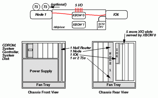
The figure above shows a one-node deskside system. It may contain either one or two processors. The single node board is installed in the node slot closest to the center of the module as viewed from the rear. This node board connects over the midplane to the first XBOW ASIC. This connection is indicated with a red line in the figure. Since only one XBOW has a node attached, only 6 XIO slots are available. These are the 3 upper and 3 lower slots closest to the center of the module. One of these, the centermost upper slot, must contain an IO6 card. The remaining 5 Half Size slots are available for other XIO cards.
Since there is only one node in the system, no router is required. To fill the slots available for routers, a board called the Null Router comes installed in the system. We will describe this board in the course of discussing the next configuration, a two-node deskside system.
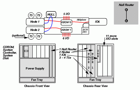
This configuration supports either 3 or 4 processors. The first node board is installed in the centermost node slot, and the second node board is installed in the slot immediately to its left as viewed from the rear of the module.
Since two node boards are installed, both XBOWs are active and thus 12 XIO slots are available. As in the one-node configuration, the first XIO slot is filled with the IO6 board; the remaining 11 slots are available for other IO options.
In order to allow the two node boards access to each other's memory, they must be connected via the CrayLink interconnect. Since there are only two nodes, they can be connected directly to each other without the use of a router chip. This configuration is shown in the diagram in the upper right hand corner of the figure. Not using a router chip to connect the two hubs reduces the time to access remote memory by about 100 nsec.
In order to physically make this connection, a Null Router board is used. This board joins together the midplane traces running from the two node board connectors to the first router board connector. This connection is indicated in the figure with a blue line; it's just a simple wire-to-wire connection. The Null Router can only be used in systems with 2 or fewer node boards. When there are more than 2 node boards in a system, routers are required to control the flow of information between hubs. The smallest configuration requiring a router is shown next.
This is a three-node deskside system. It will contain either five or six R10000 CPUs. As in the previous configurations, node boards are installed from the centermost slot outward. All 12 XIO slots are available, except for the first which holds the IO6 board.
The interesting aspect of this configuration is how the CrayLink interconnection fabric is constructed. Since there are three node boards, a simple wire-to-wire connection is not possible; a router must be used. So a Standard Router board, which contains one router chip, is installed in the first router board slot in the front of the module. As with the other boards in the system, this is the slot closest to the center of the module.
The midplane connections from nodes 1 and 2 attach to this first router board. They are shown in blue in the figure. However, the midplane connection for node 3 is wired to the second router slot. Since a router has six CrayLink connections, the best configuration possible is to have all three nodes connected to the same router chip; this means that information traveling between hubs will pass through at most one router. In interconnect parlance this is a star configuration, and a sketch of this is shown in the upper right hand corner of the figure. The question, then, is how do we create a star configuration given that node 3 is wired to the second router slot?
This is done by installing a Star Router board into that slot. This board wires together the midplane connection to node 3 and the midplane connection which joins the two router boards, thus creating the star configuration. In the diagram, this is the blue line running from node 3, through the Star Router, and ending at the Standard Router.
In addition to this internal connection, the Star Router board has an external CrayLink connector which is joined to one of the external CrayLink connectors on the Standard Router board. This is indicated in the figure by the blue line which travels to the left of the node boards.This connection is physically implemented with a very short CrayLink cable called the Star Jumper. It is not used to carry any signals in this three-node configuration.
The above figure shows the final deskside configuration: one with four nodes. This system contains either seven or eight R10000 CPUs.
Except for the extra node card, this configuration is the same as the three-node configuration. But the addition of the extra node board slightly changes the configuration of the CrayLink interconnection fabric. It is still a star configuration, but now four nodes are connected to the router. This is shown in the diagram in the upper right hand corner of the slide. The fourth connection comes by way of the Star Jumper.
Like the third node board, the fourth node board is connected to the Star Router board via the midplane. That connection is then wired to the the external CrayLink socket on the Star Router. The Star Jumper joins the Star Router's external link, and hence the fourth node board, to one of the three external links on the Standard Router board. This forms the fourth connection to the router chip on that board.
This configuration provides an 8-processor deskside system. The Standard Router board still has two external connections which have not been used, but there is no configuration available to make use of them. Expanding the system to more than 8 processors requires moving to a rack configuration.
In a rack configuration, Null Routers and Star Routers are not used. Instead, both router slots hold Standard Router boards. This produces the configuration diagrammed in the upper right hand corner of the figure below:
Each Router is connected to two node boards, and the two routers are connected to each other via one of their other CrayLink connections. All of these connections are made on the midplane in an Origin2000 module and are indicated in the figure by blue lines. This configuration contains 8 processors. Additional modules must be added to create systems with more processors.
Each router has an additional three links available for further connections. These are external links and CrayLink cables are required for them. The "Chassis Front View" on the left side of the above figure shows the three connectors on each router board to which the CrayLink cables attach.
In comparison to the star configuration on the previous slide, this configuration has a higher average latency since data traveling between the first and second node-pairs require passing through two routers instead of just one; passing through an additional router adds about 100 nsec to the cost of a memory access.
Before proceeding to configurations with more than 8 processors, we point out that rack configurations with fewer than 8 processors utililize an Origin2000 module with two routers installed; a one-node rack system is shown above. There are no rack configurations utilizing Null Routers, Star Routers, or even no routers at all. Rack modules always have a full compliment of routers for easy expansion.
When expanding a system, one generally first adds node boards to a module with available node board slots; when this module has has been filled, additional modules are added. This, however, is not a requirement; configurations can employ multiple, partially-filled modules.
Systems with more than 8 processors are built from multiple 8P12 modules. The diagram on the left of the above figure shows an Origin2000 rack module with four node boards, two routers, and two XBOWs. In the diagrams to follow, we will treat this as an atomic unit from which bigger configurations are constructed. The XBOWs are superfluous for demonstrating the CrayLink connections, so they will henceforth be omitted from the diagrams.
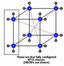
The right side of the figure shows a 16-processor system constructed from two Origin2000 rack modules. The two modules are connected by attaching CrayLink cables to form a square router configuration. This square configuration is simply a two-dimensional hypercube. We mentioned earlier that a hypercube configuration reduces the number of routers that information needs to pass through, and this keeps the system's average latency low. Since two nodes are attached to each router, this is also sometimes referred to as a bristled hypercube.
As for the physical connections, two CrayLink cables are used: one runs from one of the sockets on the first router board of the first module to the corresponding socket on the first router board of the second module; the second cable joins corresponding connectors on each module's second router board. For this 16-processor system, four of each router's links have been utilized leaving two additional links for further system growth.
Note, however, that even though we have and will continue to show larger systems constructed from complete 8P12 modules, systems do not have to have a multiple of 8 processors. A system can have any number of node boards between one and 64. In addition, while systems are generally constructed by filling up one module before adding another, this is not required. Since all 12 XIO slots in a module are activated after 2 node boards have been installed, one can configure systems which emphasize the I/O, rather than the computational, capabilities by partially populating modules with node boards.
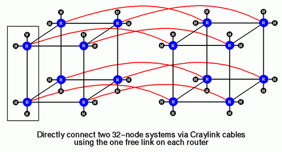
Systems with 17 to 32 processors are created from a three-dimensional hypercube of routers. This is constructed from four 8P12 modules. First, one connects pairs of modules to form 16-processor systems. Then four CrayLink cables are used to connect corresponding router pairs in the two 16-processor systems. This results in the cubic configuration shown above. Five of the six links on each router are used to produce this CrayLink interconnect configuration.
Just as with the single rack system, we don't have to completely fill up the hypercube. In the 32-processor configuration shown, imagine that the left-most 8P12 module, namely, the one inside the rectangle, disappeared along with the CrayLink connections running to it. Furthermore, imagine that the two nodes attached to the bottom router in the adjacent 8P12 module also disappeared. This now represents a 20-processor system. There are 10 node boards and 6 routers. Four of the routers utilize five of their six router links, and two utilize only four. The worst-case latency in the 20-processor system is the same as in the 32-processor system, that is, the same number of router traversals are required to communicate information between nodes which are farthest apart.
Since every router in a system with 17 to 32 processors has at least one unused CrayLink connection, the system can easily be expanded beyond 32 nodes; we'll see how this is done shortly. Alternatively, the extra link opens up the possibility of doing something to reduce the worst-case latency in the system. This can be accomplished by adding Xpress Links to the system.
Xpress Links are optional CrayLink cables which connect routers along the diagonals of the cube. These are shown as red dashed lines in the diagram. The diagonal connections reduce the worst case latency by one router traversal; this also reduces the average latency in the system. In a 4-module configuration there are four diagonals and hence four Xpress Links. In a three-module configuration, such as the 20-processor case we just discussed, there are only 2 Xpress Links since two of the routers disappear.
Note that Xpress Links can also be installed on smaller systems. For systems with two Origin2000 modules, two Xpress Links can be added along the diagonals of the square router configuration to reduce system latency. For systems containing only one module, there are no diagonals in the router configuration, so Xpress Links cannot be added.
If one wants to expand beyond 32 processors, Xpress Links cannot be installed since the extra CrayLink connection is needed to expand the router configuration. Systems with 33 to 64 processors are created from a four-dimensional hypercube of routers. This is constructed from up to eight Origin2000 modules. First, build up a 32-processor system from four modules, then add four additional modules, cabling together router pairs from the corresponding locations in the two 32-processor halves of the system. As before, for systems with fewer than 64 processors, add only as many modules as necessary.
The diagram above shows a full 64-processor system with the CrayLink cables between corresponding router pairs drawn in red.
Note that in systems of this size, all six available CrayLink connections are being used. Thus, how to expand beyond 64 processors may not be immediately obvious.
The trick that is used is shown in the figure below: instead of using a simple hypercube, we change to a hierarchical hypercube.
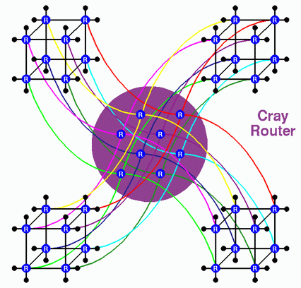
A 128-processor system starts with four 32-processor systems. The routers in each of these systems have one available CrayLink connection. Instead of connecting pairs of spare links directly to each other, we connect quads of corresponding routers. We cannot directly connect four CrayLinks together, so we add 8 additional routers to the system and connect each quad to one of them. The connections to each of these additional routers forms a star, just as we saw earlier when describing the 4-node deskside configuration. These additional routers are not connected to nodes or to each other; they only attach to the corresponding corner of each of the four 32-processor systems.
In the above diagram the 8 additional routers are surrounded by the four, 32-processor cubes. The four connections of the star are easily seen for the upper right router; these connections are drawn in red. From this diagram, one can see that communication within this configuration requires the same number of router traversals as is needed by a 5-dimensional bristled hypercube. To construct the hypecube, however, would require routers with 7 links, whereas this configuration is made up of 6-link routers.
The 8 additional routers come in a separate piece of hardware called the Cray Router. This must be configured into systems with more than 64 processors. Physically, it is comprised of two rack-mount modules which fill one rack. Each module houses four Cray Router boards. These differ from Standard Router boards in that they have 4 sockets on the edge, rather than three, in order to make the four required cable connections.
Expansion beyond 128 processors is supported by connecting together multiple Origin2000 systems into an array.
We conclude the discussion of the architecture of the Origin2000 system by summarizing the bandwidths and latencies of different size systems. These are shown in the following table:
| Configs | Memory & I/O | Interconnect Bandwidths | Routers | Read Latencies | |||||
| XBOWs:Nodes:CPUs | Max | Avg | Max | Avg | |||||
| Memory | I/O | Total Bisection BW | BBW/Node | BBW/CPU | # | # | ns | ns | |
| 1:1:2 | .78 | 1.56 | - | - | - | - | - | 313 | 313 |
| .68 | 1.25 | - | - | - | |||||
| .59 | |||||||||
| 2:2:4 | 1.56 | 3.12 | 1.56 | .78 | .39 | - | - | 497 | 405 |
| 1.37 | 2.50 | 1.25 | .62 | .31 | |||||
| 1.19 | |||||||||
| 2:4:8 | 3.12 | 6.24 | 3.12 | .78 | .39 | 1 | .75 | 601 | 528 |
| 2.73 | 4.99 | 2.50 | .62 | .31 | |||||
| 2.38 | |||||||||
| 4:8:16 | 6.24 | 12.48 | 6.24 | .78 | .39 | 2 | 1.63 | 703 | 641 |
| 5.47 | 9.98 | 4.99 | .62 | .31 | |||||
| 4.75 | |||||||||
| 8:16:32 | 12.48 | 24.96 | 12.48 | .78 | .39 | 3 | 2.19 | 805 | 710 |
| 10.94 | 19.97 | 9.98 | .62 | .31 | |||||
| 9.50 | |||||||||
| 16:32:64 | 24.96 | 51.2 | 12.48 | .39 | .2 | 5 | 2.97 | 908 | 796 |
| 21.87 | 39.94 | 9.98 | .31 | .16 | |||||
| 19.00 | |||||||||
| 32:64:128 | 49.92 | 99.84 | 24.96 | .39 | .2 | 6 | 3.98 | 1112 | 903 |
| 43.74 | 79.87 | 19.97 | .31 | .16 | |||||
| 38.00 |
In this table multiple values are provided for the bandwidths (all values are for 195 MHz systems). The top value is the raw bandwidth supported by the physical connections. The second value is the peak bandwith reduced by the amount consumed by control overhead; this is the maximum bandwidth available to user data. For memory bandwidths, a third value is also provided. This is the peak read bandwidth from local memory.
The first column of the table shows the system configurations; these are categorized by the number of XBOWs, nodes and processors. The next two columns then show the memory and I/O bandwidth foor each of these configurations. Memory bandwidth scales linearly with the number of nodes. One might expect that I/O bandwidth would scale linearly with the number of XBOWs. But since a XBOW can connect to two nodes, the I/O bandwidth per XBOW will double when two nodes are connected as compared to just one. Thus, I/O bandwidth also scales linearly with the number of nodes.
The next three columns detail the bandwidths of the interconnection fabric. The basic unit of measure is the bisection bandwidth. This is a measure of the total amount of communication bandwidth the system supports. Due to the hypercube topology of the router configuration, it essentially scales linearly with the number of nodes. There is one anomoly observed between 32- and 64-processor systems. For these two configurations, the total bisection bandwidth is the same. This is because the figures in this table reflect the use of Xpress Links for the 16- and 32-processor configurations, which provides extra bandwidth. (In addition, the highest bandwidth configurations have been used for the smaller sized machines; namely, a star router is used for the 8-processor configuration and a null router is used for the 4-processor configuration.) The second and third bisection bandwidth columns show how the bisection bandwidth varies on a per-node and per-processor basis. An ideal communication infrastructure would allow constant bisection bandwidth per node or cpu, and this is what is observed, except for the step which results from changing from Xpress Link configurations to non-Xpress Link configurations.
The next two columns show the maximum and average number of router traversals for each configuration. The maximum hops figure grows as the base-2 logarithm of the number of processors, except for a jump of 1 when transitioning from 32 processors with Xpress Links to 64 processors without them. The average number of router hops is calculated by averaging over all node-to-node paths. For example, the 8-processor star router configuration has 4 nodes. Each node can access its own memory with 0 router hops, but it takes 1 router hop to get to any of the three remote memories. The average number of hops is thus 0.75.
The final two columns show maximum and average read latencies. This latency is the time to access the critical word in a cache line read in from memory. For local memory accesses, the maximum latency is 313 nsec. For a hub-to-hub direct connection (i.e., a two-node configuration), the maximum latency is 497 nsec. For larger configurations, the maximum latency grows approximately 100 nsec for each router hop. Average latency is calculated by averaging the latencies to local and all remote memories. What is amazing is that even for the largest configuration, 128 processors, the average latency is no worse than on Power Challenge systems, demonstrating that shared memory can be made scalable without negatively affecting performance.
In this section we describe the architecture of the R10000 microprocessor.
The R10000 is the latest microprocessor from MIPS Technologies. It is designed to solve many of the performance bottlenecks common in existing microprocessor implementations. In the Origin2000, the R10000 runs at either 195 MHz or 180 MHz.
The R10000 is a 4-way superscalar RISC processor. It can fetch and decode 4 instructions per cycle to be scheduled to run on its five independent, pipelined execution units: a non-blocking load store unit, 2 64-bit integer ALUs, a 32-/64-bit pipelined floating point adder, and a 32-/64-bit pipelined floating point multiplier. The integer ALUs are asymmetric. While both carry out add, subtract, and logical operations, ALU 1 handles shifts, conditional branch and conditional move instructions, while ALU 2 is responsible for integer multiplies and divides. Similarly, instructions are partitioned between the floating point units. The floating point adder is responsible for add, subtract, absolute value, negate, round, truncate, ceiling, floor, conversions and compare operations, and the floating point multiplier carries out multiplication, division, reciprocal, square root, reciprocal square root and condtional move instructions; the two units can be chained together to perform multiply-add and multiply-subtract operations.
Instruction latencies are presented in the following table:
Instruction Type        Ex Unit Latency Repeat  Comment
-------------------------------------------------------------------------------
                        Integer instructions
-------------------------------------------------------------------------------
Add/Sub/Logical/Set     ALU 1/2 1       1
MF/MT HI/LO             ALU 1/2 1       1
Shift/LUI               ALU 1   1       1
Cond. Branch Evaluation ALU 1   1       1
Cond. Move              ALU 1   1       1
MULT                    ALU 2   5/6     6       Latency relative to Lo/Hi
MULTU                   ALU 2   6/7     7       Latency relative to Lo/Hi
DMULT                   ALU 2   9/10    10      Latency relative to Lo/Hi
DMULTU                  ALU 2   10/11   11      Latency relative to Lo/Hi
DIV/DIVU                ALU 2   34/35   35      Latency relative to Lo/Hi
DDIV/DDIVU              ALU 2   66/67   67      Latency relative to Lo/Hi
Load (not to CP1)       Ld/St   2       1       Assuming cache hit
Store                   Ld/St   -       1       Assuming cache hit
-------------------------------------------------------------------------------
                        Floating-Point instructions
-------------------------------------------------------------------------------
MTC1/DMTC1              ALU 1   3       1
Add/Sub/Abs/Neg/Round
  Trunc/Ceil/Floor/
  C.cond                FADD    2       1
CVT.S.W/CVT.S.L         FADD    4       2       Repeat rate is on average
                                                Repeat pattern: IIxxIIxx...
CVT (others)            FADD    2       1
Mul                     FMPY    2       1
MFC1/DMFC1              FMPY    2       1
Cond. Move/Move         FMPY    2       1
DIV.S/RECIP.S           FMPY    12      14
DIV.D/RECIP.D           FMPY    19      21
SQRT.S                  FMPY    18      20
SQRT.D                  FMPY    33      35
RSQRT.S                 FMPY    30      20
RSQRT.D                 FMPY    52      35
MADD                    FADD+                   Latency 2 only if the result is
                        FMPY    2/4     1       used as addend of another MADD
LWc1/LDC1/LWXC1/LDXC1   Ld/St   3       1       Assuming cache hit
The R10000 implements the MIPS IV instruction set architecture (ISA). This is a superset of the previous MIPS I, II and III ISA's, so programs compiled for those ISA's are binary compatible with the R10000. The MIPS IV ISA is also used in the R8000, so R8000 programs as well are binary compatible with the R10000.
In addition to the 32- and 64-bit instructions contained in the previous MIPS ISA's, MIPS IV also includes floating-point madd (multiply-add), reciprocal, and reciprocal square root instructions, indexed loads and stores, prefetch instructions, and conditional moves. While MIPS I, II, and III load and store operations allow addresses to be constructed as a compile-time constant offset from a base register, indexed loads and stores allow the offset to be a run-time value contained in an integer register; these instructions allow one to reduce the number of address increments inside loops. Prefetch instructions allow one to request data to be moved into the cache well before it is needed, thus eliminating much of the latency of a cache miss. Conditional move instructions can be used to replace branches inside loops, thus allowing tight, superscalar code to be genrated for those loops. The MIPS IV ISA specifies the availablility of 32 integer and 32 floating-point registers.
The R10000 has a two-level cache hierarchy. Located on the microprocessor chip are a 32 KB, 2-way set associative level-1 instruction cache and a 32 KB, 2-way set associative, 2-way interleaved level-1 (L1) data cache. Off-chip is a 2-way set associative, unified (instructions and data) level-2 (L2) cache. This secondary cache may range in size from 512 KB to 16 MB; the size of the secondary cache in the Origin2000 is 4 MB for 195 MHz systems, and 1 MB for 180 MHz systems.
The L1 instruction cache utilizes a line size of 64B, while the L1 data cache has a line size of 32B. The line size of the L2 cache may be either 64B or 128B; in the Origin2000 it is 128B. Both the L1 data cache and the L2 unified cache employ a least recently used (LRU) replacement policy for selecting in which set of the cache to place a new cache line.
The secondary cache may be run at a handful of speeds ranging from the same speed as the processor down to one third of that frequency. In the Origin2000 the secondary cache operates at two thirds the processor frequency.
The R10000 is nearly unique in allowing for a set associative off-chip cache. To provide a cost-effective implementation, however, only enough wires are provided to check for a cache hit in one set of the secondary cache at a time. To allow for 2-way functionality, an 8192-entry way-prediction table is used to record which set of a particular cache address was most recently used. This set is checked first to determine whether there is a cache hit. This takes one cycle and is performed concurrently with the transfer of the first half of the set's cache line. The other set is checked on the next cycle while the second half of the cache line for the first set is being transferred. If there is a hit in the first set, no extra cache access time is incurred. If the hit occurs in the second set, its data must be read from the cache, and a minimum 4-cycle mispredict penalty is incurred.
Both level-1 and level-2 data caches are non-blocking. That is, the processor does not stall on a cache miss. Up to 4 outstanding cache misses from the combined two levels of cache are supported. Cache miss latency to the second level cache depends on the speed at which that cache is run. Below is a table of some of these miss times:
Processor Speed            Latency          Repeat Rate
---------------                         (data/instruction)
   L2 Speed             (PClk Cycles)      (PClk Cycles)
-----------------------------------------------------------
       1                      6                 2/4
      1.5                   8--10               3/6
       2                    9--12               4/8
In this table the latencies assume that the way was predicted correctly and that there are no conflicting requests. The variability in the latencies for the slower cache speeds is due to clock synchronization effects. The repeat rate is the number of processor cycles needed to transfer 1 cache line to a primary cache; it takes twice as long for the L1 instruction cache as for the L1 data cache since the instruction cache line is two times as long. The repeat rate is valid for 2 to 3 cache misses; if more than three consecutive cache misses occur, an extra 1-cycle "bubble" may occur in the pipeline.
In addition to the instruction and data caches, the R10000 also has a Translation Look-aside Buffer (TLB) for holding mappings between virtual and physical addresses. This cache is fully associative and holds 64 entries, each of which maps two consecutive virtual pages. The R10000 supports variable page sizes, ranging from 4 KB to 16 MB in powers of 4. The minimum page size in Irix 6.4 is 16 KB, and the operating system can use two different page sizes. By default, about 20% of the pages are 64 KB in size, however the system administrator may change both this percentage and which large page size is available. In Irix 6.4 six of the 64 mapping slots are reserved by the operating system, so 58 are available for user programs.
As mentioned above, the R10000 is designed to solve many of the performance bottlenecks common in existing microprocessor implementations. The chief performance bottleneck is latency due to poor memory locality. The R10000 uses register remapping, out-of-order execution, and speculative execution in conjunction with its non-blocking caches to try to hide this latency.
From the programmer's point of view, instructions are executed one after another in program order, and when the output of an instruction is written into its destination register, it is immediately available for use in subsequent instructions. However, pipelined, superscalar processors may execute several instructions concurrently, and the result of a particular instruction may not be available for several cycles. Often, the next instruction in program order must wait for its operands to become available, while later instructions are ready to be executed.
The R10000 overcomes this performance bottleneck by dynamically executing instructions as their operands become available. This out-of-order execution is invisible to the programmer: any result which is generated out of order is temporary until all previous instructions have been completed. If an exception is generated by a previous instruction, all temporary results can be undone and the processor state returned to what it would have been had the instructions been executed sequentially. If no exceptions occur, an instruction executed out of order is "graduated" once all previous instructions have completed, and its result is added to the visible state of the processor.
In order to permit out-of-order execution, register renaming is performed. Typically, the register names used in a program's instructions are the same as the physical registers in the processor. This need not be the case. The names used in the instructions can be treated as logical names, and these can be mapped to physical names in any way which is useful. In particular, logical registers can be renamed to avoid instruction dependencies.
Since there may be an indeterminate amount of latency required to complete a given instruction (for example, an input value may depend on a cache miss), execution of subsequent instructions in the program may be delayed if the name of an output register is the same as one used in a latency-stalled instruction. Instead of waiting to overwrite a register of a particular logical name, the processor may select any available physical register to use in its place, thus allowing later instructions to executed without delay.
The R10000 renames all logical result registers as instructions are decoded, and renames the physical result registers back to their logical names once each result is committed to the processor state. Up to 32 instructions may be active in the processor at a given time, enough to hide at least 8 cycles of latency. These instructions are tracked in the Active List: instructions are added to the Active List when they are decoded, and they are removed upon graduation. In order to have enough room for both temporary and committed results, there are more physical registers than logical registers. The R10000 has 64 physical integer registers and 64 physical floating-point registers, enough to allow 32 committed results and 32 temporary results in the Active List. Free lists --- one for the integer registers and one for the floating-point registers --- are maintained to track which physical registers are available to be used in place of a logical register; registers are taken off the free list as instructions are decoded, and they are returned when instructions graduate.
Queues are used to select which instructions to issue dynamically to the execution units. Three separate 16-entry queues are maintained: an integer queue for ALU instructions, a floating-point queue for FPU instructions, and an address queue for load and store instructions. Instructions are placed on the queues when they are decoded. Integer and floating-point instructions are removed from their respective queues once the instructions have been issued to the appropriate execution unit; load and store instructions remain in the address queue until they graduate since these instructions can fail and may need to be reissued; for example, a data cache miss or a way misprediction will require the instruction to be reissued.
In addition to exceptions generated by previous instructions, there is one other reason for undoing temporary results. The R10000 executes instructions speculatively upon encountering a conditional branch instruction. That is, it predicts whether or not the branch will be taken and fetches and executes subsequent instructions accordingly. If the branch prediction is correct, then execution will have proceeded without interruption. If the prediction was incorrect, however, then any instructions executed down the incorrect program path must be cancelled, the processor must be returned to the state it was in when it encountered the mispredicted branch, and execution continues with the correct path.
The R10000 may speculate on the direction of branches nested four deep. In order to predict whether or not to take the branch, a 2-bit algorithm, based on a 512-entry Branch History Table, is used. Simulations have shown the algorithm to be correct 87% of the time on the SpecInt92 suite.
The details of how register renaming, out-of-order execution, and speculative execution in the R10000 works can be demonstrated with a simple example. Below is a code fragment and details of the register renaming that occurs when it is run. Each logical output register is mapped to a different physical register. Doing so removes false dependencies such as are seen in instruction 4 for logical register r3.
       Assembly Code           Physical Operation      Rename  Unit    Cycle   Comments
------------------------------------------------------------------------------------------------------------------
1      DSLL    r3,r2,2         p9 <-p2 shift left 2    r3=p9   ALU1    1A
2      LW      r4,0x8(r3)      p10<-mem(p9+8)          r4=p10  L/ST    1B      true dependency "r3" on inst #1
3      ADD1    r5,r2,0x34      p11<-p2+'34'            r5=p11  ALU     1C
4      SUB     r3,r1,r5        p12<-p1-p11             r3=p12  ALU     1D      true dependency "r5" on inst #3
                                                                               output dependency "r3" on inst #1
                                                                               anti dependency "r3" on inst #2
5      XORI    r2,r1,0xFF      p13<-p1 xor 'FF'        r2=p13  ALU     2A
6      BEQ     r4,r2,label     branch if p10=p13       none    ALU1    2B      conditional branch (predict taken)
7      NOP     -               no operation            none    ALU     2C      delay slot (instr after branch)
8      MULT    r3,r4                                                           (not decoded if branch is taken)
9      MFLO    r2,....
...........
label:
10     AND     r3,r1,r2        p14<-p1 and p13         r3=p14  ALU     3A
11     LB      r4,0(r3)        p15<-mem(p14+0)         r4=p15  L/ST    3B
This example also has a branch at instruction 6. We will assume that the branch is predicted to be taken; thus, execution will jump from the branch delay slot at instruction 7 to the branch target at instruction 10. This execution will be speculative since the condition determining which direction the branch should really go cannot be evaluated until a few cycles after the branch is encountered.
Here is a schematic showing a cycle-by-cycle account of the events occurring inside the processor as this code fragment is run. During cycle 1, the first 4 instructions are fetched and decoded. In cycle 2, instruction 1 is issued since it has no dependencies. Instruction 2 depends on the result of instruction 1, so it must wait to issue. Instruction 3 has no dependencies, so it may issue. Instruction 4 depends on the result of instruction 3, so it must wait. Finally, instructions 5 through 7 are fetched and decoded in this cycle. Due to the branch at instruction 6, instructions following the delay slot that are not in the predicted direction are not decoded, so only 3 instructions are decoded during this cycle.
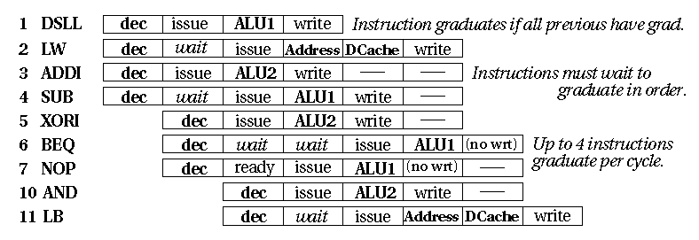
In cycle 3, instructions 1 and 3 are executed by ALU1 and ALU2, respectively. Instructions 2 and 4 are issued since there is only a 1 cycle latency needed to complete the instructions they depend upon. Instruction 5 also issues since it has no dependencies. Instruction 6 must wait since it depends on the result of instruction 5. Instruction 7 is ready to issue, but the two ALUs will be busy working on previous instructions during the next cycle, so its issue is delayed. Fetch and decode resumes with instructions at the predicted target of the branch at instruction 6.
In cycle 4, the results of instructions 1 and 3 are written to the register file. These are used by instructions 2 and 4 as they execute in the address unit and ALU1, respectively. Since ALU2 is available, instruction 5 also executes. Since the branch at instruction 6 depends on the result of the load in instruction 2, it must wait another cycle before issuing since the result of instruction 2 will not be written before cycle 6. This allows instructions 7 and 8 to issue in preparation for being executed in the ALUs on the next cycle. Instruction 9 depends on the result of instruction 8, so it needs to wait one cycle before issuing.
In cycle 5, instruction 1 may graduate if all previous instructions have done so. Instruction 2 accesses the primary dcache to load a word. If the cache access is a hit, the loaded word will be available in a register during cycle 6; if the load misses, instruction 6, which depends on the value, will have to wait for the value to come from the secondary cache or main memory. This example assumes a primary cache hit. Instructions 4 and 5 write their results to the register file, instructions 7 and 8 execute in the ALUs, and instructions 6 and 9 issue since they have no more dependencies to wait for. Instruction 3, although complete, must wait to graduate since instructions must graduate in order, and instruction 2 is still not complete.
In cycle 6, instruction 2 writes its result to the register file where it can be used by instruction 6 which is now executing in ALU1. Instructions 3, 4 and 5 are all complete, but they need to wait for instruction 2 before they can graduate. Instructions 7 and 8 are in the write stage of the execution pipeline, but instruction 7 does no write since it is a NOP. Instruction 9 now executes in the address unit since the value it depends on is being written into the register file by instruction 8.
On cycle 7, instruction 2 is complete. Since it is the oldest instruction active, it graduates first. Instructions 3, 4 and 5 may also now graduate. Only 4 instructions per cycle may graduate, so no other instructions would have graduated had they been ready to do so. The result of instruction 6 is now available, so the processor can determine if the branch prediction was correct. If it was not, instruction 9 would need to be aborted and the result of instruction 8 would have to be thrown away. In this example, we assume the prediction was correct. Instructions 7 and 8 are complete, but they must wait one more cycle for instruction 6 to complete before they can graduate. Instruction 9 accesses the primary dcache to load its value.
On cycle 8, instruction 6 has completed, so it and instructions 7 and 8 may graduate. Instruction 9 writes its result to the register file, assuming a hit in the dcache.
The ability to execute instructions out-of-order, combined with the non-blocking caches, allows the the R10000 to hide the latency associated with many cache misses. The Active List can hold up to 32 instructions, so at least 8 cycles of latency can be hidden. This is enough to cover much of the latency from the secondary cache, but is still well short of that needed to cover the latency from main memory accesses.
The speculative execution enabled by the R10000's branch prediction allows it to run branch-laden code efficiently. This hardware approach is quite different than the software approach required in other superscalar processors. For example, the R8000 does minimal speculation in hardware. In order to efficiently run loops which contain conditional constructs such as if-then-else, the compiler must replace the branches these constructs normally produce with conditional moves. To do so the compiler may cause the processor to evaluate both the then and else clauses of the if statements. This software speculation allows tight code to be generated for the loop, but it also causes the processor to execute more code. Furthermore, generating and executing code for clauses that should be skipped can cause exceptions, which need to be handled by operating system traps. Such software speculation is generally not needed for the R10000, and in fact, is often counter-productive, slowing down execution time in comparison to the hardware speculation which is automatically performed.